Background
Atomic layer deposition (ALD) is the best technique for producing films with nanometre-scale thickness control, as it deposits a film one atomic layer at a time. As feature sizes continue to decrease in applications such as integrated circuits and memory devices, ALD is becoming the only option for depositing some thin-film components which are not possible using CVD and PVD processes.
Conventional ALD operates by sequentially inserting two chemical precursor gases into a vacuum chamber, with evacuation and purge steps in between the exposures. A single atomic layer of the material is formed after each sequence, and the sequence is repeated multiple times to build up a film. Hence conventional ALD separates the two precursor gases in time. In contrast, spatial atomic layer deposition (SALD) techniques have been developed, which separate the two precursors in space, rather than in time. The substrate is moved back and forth between the two precursor gases to replicate the sequential exposures. This eliminates the evacuation and purge steps that make SALD slow. Since it can operate in atmospheric conditions, it is often referred to as atmospheric pressure spatial ALD (AP-SALD). AP-SALD can produce thin-film layers of materials (typically metal oxides) that are compact and pinhole-free. AP-SALD can deposit thin films at low temperatures (typically 100 to 350°C), is 1-2 orders of magnitude faster than conventional ALD, and is scalable (roll-to-roll compatible).
Description of the invention
University of Waterloo (UW) researchers have developed a novel commercial-scale AP-SALD system that aims to upscale lab devices (~1 cm2) to commercial-scale devices (>232 cm2) while maintaining and improving their efficiency, stability, and uniformity. This system enables high-throughput manufacturing that facilitates the commercialization of next-generation nanomaterials.
Advantages
- Deposition process operates in ambient pressure, eliminating the high operational and capital cost associated with vacuum-based methods in existing ALD, CVD, PVD technologies.
- Ability to deposit controlled and conformal nanoscale films, including sub-10 nm films as well as films >20 nm thick with ~1 nm resolution.
- Modular design to allow scaling for high throughput (>1000 wafers/ hr possible) and deposition over large areas (i.e., > 15 cm x 30 cm).
- Capacity to deposit different materials (e.g., SnO2, WO3, Al2O3, AZO…) on a wide range of substrate types, thickness, and geometries.
- Low temperature deposition is compatible with flexible substrates
Potential applications
- Thin film electronics including memory devices, logic chips, power electronics, display technologies, smart fabric, smart windows.
- Energy storage/generation including batteries, battery electrode, fuel cells, solar cells, thermoelectric devices.
- Flexible electronics and sensor applications within the automotive, environment and medtech sectors.
- Emerging devices and MEMS/NEMS, such as nanotube/nanowire devices, graphene/carbon nanotube devices, optoelectronics.
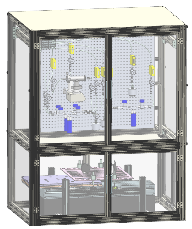
Figure 1. Spatial ALD System
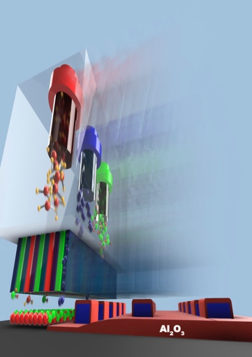
Figure 2. Conformal coating by SALD
Reference
10165
Patent status
US Provisional Patent filed
Stage of development
Working Prototype validating system
capacity/throughput and material capabilities
Contact
Scott Inwood
Director of Commercialization
Waterloo Commercialization Office
519-888-4567, ext. 43728
sinwood@uwaterloo.ca
uwaterloo.ca/research