The Waterloo Institute for Nanotechnology and the Department of Electrical and Computer Engineering presents
High Aspect Ratio Polymer and Metal Patterning at the Synchrotron Laboratory for Micro and Nano Devices (SyLMAND), Canadian Light Source
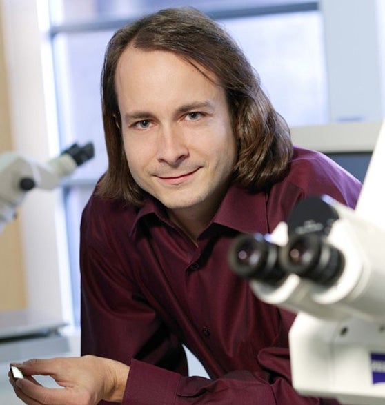
Dr. Sven Achenbach
Department of Electrical and Computer Engineering
University of Saskatchewan
Monday, July 15, 2019
3:30 - 4:30 p.m.
QNC 1501
All are welcome to attend.
Abstract:
Deep X-ray lithography (XRL) complements other micro and nano fabrication processes available in Canada. While many patterning processes traditionally target highest lateral resolution in shallow films and often focus on silicon materials, XRL is commonly optimized for the patterning of thick resist layers (typically, up to hundreds of micrometers or even millimeters) with high aspect ratios (ratio of thickness to minimum lateral feature size; up to 100:1), and smooth and vertical sidewalls, at reduced requirements on lateral resolution. XRL can be combined with subsequent process steps of the LIGA process (German acronym for lithography, electroplating, and replication) to obtain a wider variety of patterned materials (including polymers, metals and ceramics) and to reduce the cost per patterned component by mass replication rather than individual lithography. In Canada, XRL has recently become available to the scientific community and to industrial users as SyLMAND, the Synchrotron Laboratory for Micro and Nano Devices of the Canadian Light Source (CLS) in Saskatoon, became operational. The talk will give a brief introduction to XRL processing, explain some of SyLMAND’s unique contributions to XRL instrumentation and technology, and highlight selected applications in the areas of vertical wall radio frequency (RF) MEMS and antennas, X-ray optics, and fluidics.