What does WATLab stand for?
“WATLab” stands for “Waterloo Advanced Technology Lab”. We highlight the primary mission of the Laboratory here, which is to develop advanced technology applications through innovative fundamental research. For more info, go to www.watlab.com.
When was WATLab established and where does its money come from?
WATLab was established as a multidisciplinary materials characterization and fabrication research centre at Waterloo in early 2000. Its $20 M equipment capital was provided by the Canada Foundation for Innovation and the Province of Ontario through four Institutional Innovation Awards. It is one of the very few centres fortunate enough to receive this support multiple times at Waterloo, and it shows the Governments’ commitments to advanced technology through investments in innovative fundamental and applied research.
Its on-going operating cost is being supported by user fees, and in part by my own research grants from the Natural Sciences and Engineering Research Council (NSERC) and other sources. In the past, WATLab was awarded two Major Facility Access Grants by NSERC to help to establish it as a major regional research centre in Canada’s Technology Triangle.
Over the past 15 years and despite the lack of a sustained budget, WATLab has established itself as one of the most efficiently run, state-of-the-art materials research centres in North America. In the past 10 years, we routinely operate with over 90% up time, and we have a lot of tools. About 5 years ago, we conducted a user survey of WATLab’s performance. Over 95% of the responses indicate that the users were either fully satisfied or highly satisfied with WATLab’s service and performance. Almost all have indicated that if WATLab were to shut down tomorrow due to lack of operating funds, their research would suffer serious set-back.
What are the tools and services offered by WATLab?
WATLab offers a “complete” fleet of state-of-the-art instrument systems for materials characterization and fabrication second to none in Canada. Many of our tools are not only state-of-the-art but indeed unique, and they include:
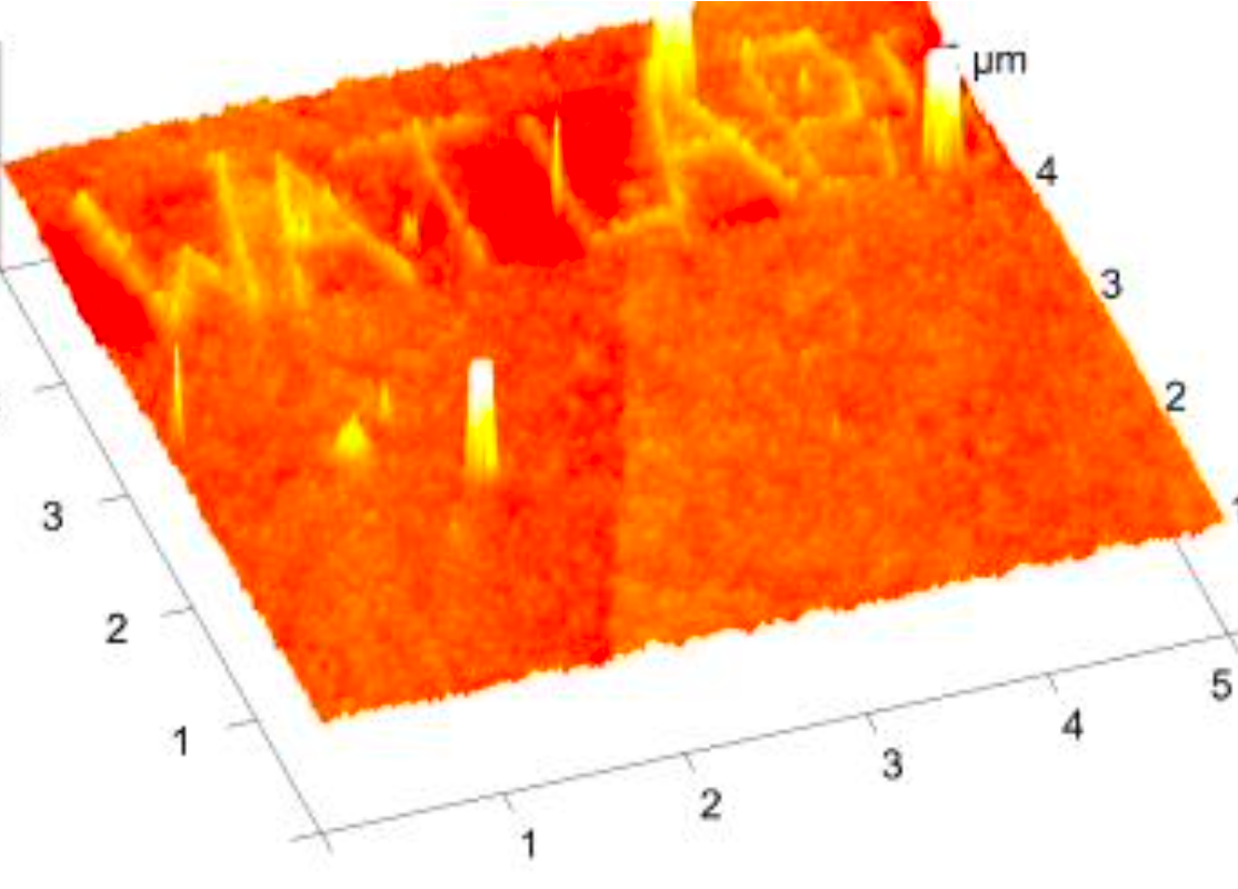
- All areas of microscopy and structural determination tools, including three field-emission Scanning Electron Microscopes, and more recently an Environmental SEM, TEM, Canada’s first Helium Ion Microscopy, AFM, STM, and dual-beam focussed ion beam system. We also have X-ray diffractometers (one for powders and one for thin film work) and a small-angle X-ray scattering system.
- All areas of spectroscopies, including electron spectroscopy (ESCA or XPS, Scanning Auger Microscopy), optical spectroscopies (from IR and Raman to UV and PL), and a Time-of-Flight Secondary Ion Mass Spectrometry system.
- Bulk characterization tools that include both PPMS (physical property measurement system) and MPMS (magnetic property measurement system such as SQUID).
- Material and device prototyping. In the past few years, we have aggressively set up new tools in this area, including some unique lithography and nanopatterning tools such as Maskless Optical Lithography, Electron Beam Lithography, and Canada’s first Ion Beam Lithography system.
Who are the WATLab users?
WATLab has a broad user base. We have over 100 research groups, from 9 departments from both the Faculty of Science and the Faculty of Engineering at Waterloo. Currently, we have 45 active user groups, with over 100 students, postdoctoral fellows and senior researchers, using our facilities. Our staffs also provide regular training sessions for some of our tools, e.g. our SEM, and we assist users with their on- going research.
We currently have about 20 industrial users, mostly from the immediate Kitchener-Waterloo-Cambridge and Guelph areas. We occasionally have users from as far as the west coast, the United States and even India.


What is the ongoing research at WATLab?
Our users are conducting exciting research, from new nanomaterials for green energy applications, to catalysts for oil sand refineries, to remediation technologies for water research, to flexible electronics for next-generation wearable devices, to quantum materials for quantum computers. In my group, we focus on three core application areas.
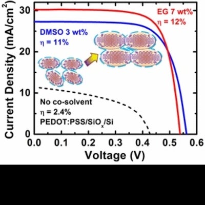
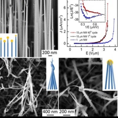
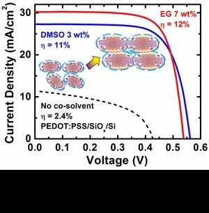
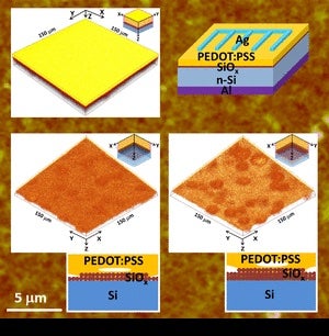
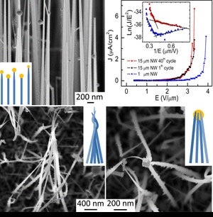
- We have on-going experiments on green energy that involve development of nanoclusters and one-dimensional nanostructures for hydrogen generation by photoelectrochemical water-splitting reaction, and new materials and strategies for inorganic, organic and hybrid solar cells. Some of our solar cells have held world-record in photoconversion efficiency.
-
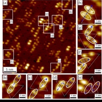
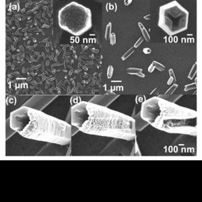
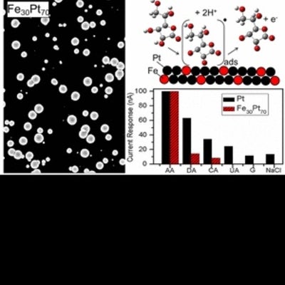
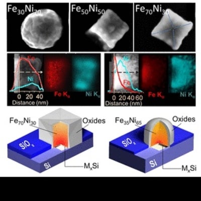
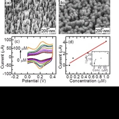
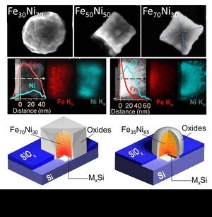
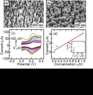
Our second series of work is the development of hybrid nanomaterials for biosensing and water remediation. These “hybrid” materials are unique and they are usually built by combining, in some clever ways, two or more nanomaterials, two or more crystalline phases or defects, two or more morphologies and physical structures. These hybrid materials offer new properties that individual component materials do not have.
-
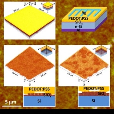
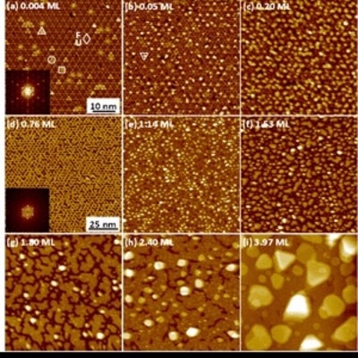
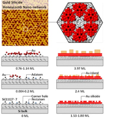
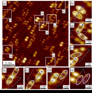
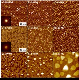
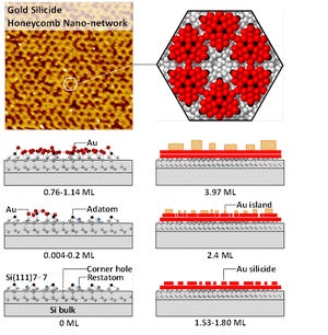
The third line of studies is the fabrication of quantum materials and nanodevices for quantum electronics applications. We have been using Molecular Beam Epitaxy to build ultrathin metallic- bio/organic-semiconductor structures, which are commonly known as MIS (or metal insulator semiconductor) devices. These nanometer-thick device architectures provide a novel platform for site-specific chemistry and processes not possible before, and they could be used for molecular trapping and advanced surface functionalization. We also have unique tools such as Canada’s first Helium Ion Microscope, Canada’s first Ion Beam Lithography system, Canada’s first nanocluster source, and Canada’s first NanoPLD system. These tools are used to fabricate new electronic circuits at the nanoscale and in three dimensions, involving novel components such as memristers, phase- change memory devices, and spintronics.