
The University of Waterloo Nanotechnology program provides students state-of-the-art teaching facilities. This includes a clean room and metrology suite furnished with multi-million dollar micro- to nano-scale device fabrication and analytical equipment. Here are some of the highlighted instruments (click the image to enlarge and view the slideshow).
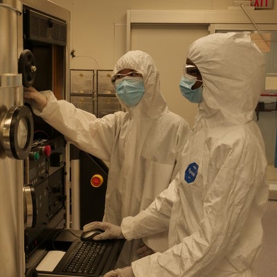
Plasma-Enhanced Chemical Vapor Deposition and Reactive Ion Etch Chambers/ Plasma Enhanced Chemical Vapor Deposition is used for the deposition of dielectric thin films. This highly specialized equipment is a type of plasma etch technology.
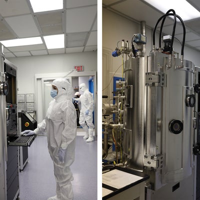
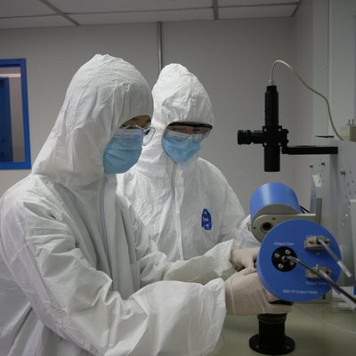
Physical Vapor Deposition Chamber/ This is cutting edge technology is used in the creation of a vaporization coating. These processes are used to deposit films with thickness of a few nanometers to thousands of a nanometers.
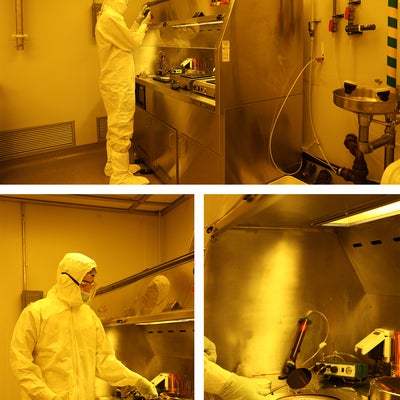
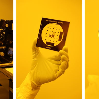
Photoresist spin coating and baking stations/ These pictures were taken in the Photolithography Room or yellow room. In this process photosensitive material is applied to a mask it is then baked so that it solidifies and transfers the pattern of the device to the wafer.
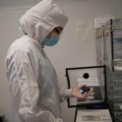
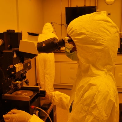
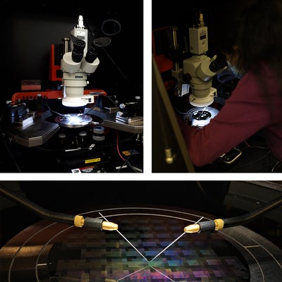
A technician inspects the wafer under a specialized microscope. The technician examines the pattern of devices that are transferred to the wafer. Four layers of mask are applied to each wafer.
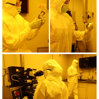
The technician visually examines the pattern of devices that are transferred to the wafer. The wafer is then further examined in more detail using a state-of-the-art microscope. UV light is also used in the yellow room. It's a sophisticated system designed to add and then inspect the different layers of masks adhered to the wafer.
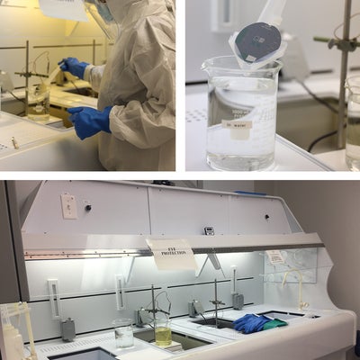
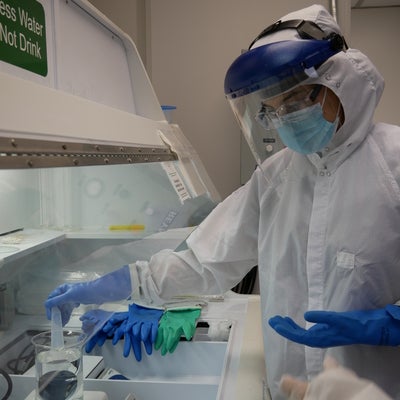
The clean room is equipped with state-of-the-art fume hoods. This is a controlled environment that redirects fumes out and away from technicians working with various solutions. Temperature checks are done with thermometers and wafers are loaded and dipped into solutions.
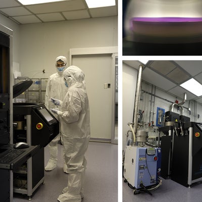
The top two pictures are of the probe station. Here the reaction of accelerated electrons are observed. The bottom picture is an ellipsometer which is used to measure the thickness of the film on the wafer.
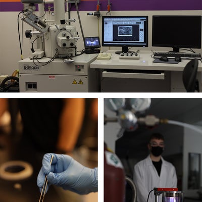
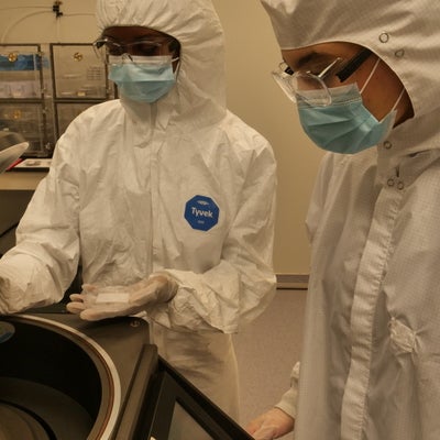
Nanotechnology Engineering labs are equipped with cutting-edge technology such as this Scanning Electron Microscope and silver sputter coater. Nano material is loaded on circular samples then loaded into the vacuum chamber. The electronic gun separates electrons from the sample and collects it.


