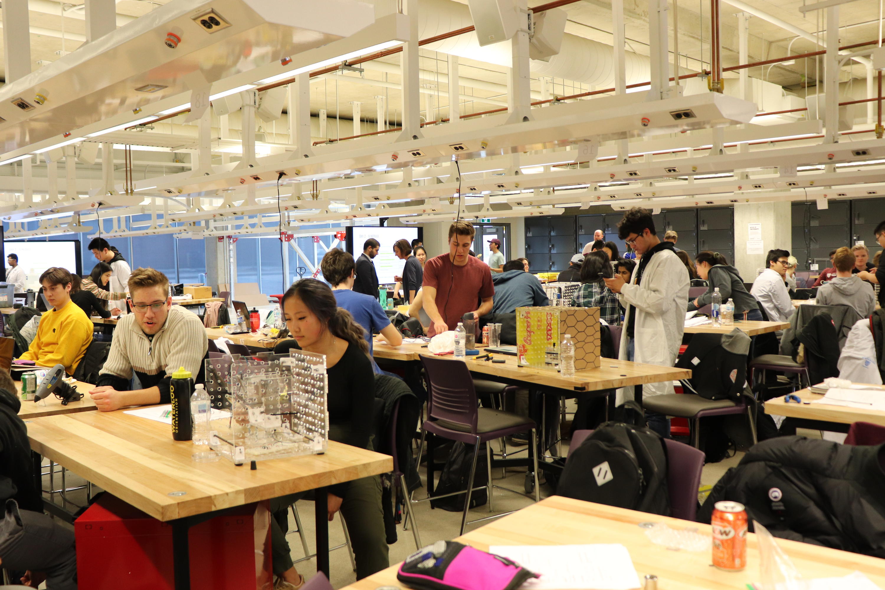
The Nanotechnology Engineering program held its first Design Days event on March 12 and 19, 2019.
Held in collaboration with the Engineering IDEAs Clinic, NE Design Days challenged teams of first-year students to work together, applying information learned throughout their first-year courses, new lecture material and a set of instructions to design, build and test their own small-scale scanning tunneling microscopes.
Scanning Tunneling Microscopes
The STM, invented in 1982, allowed researchers to view materials at the atomic level and earned inventors Gerd Binning and Heinrich Rohrer the 1986 Nobel Prize in Physics. The equipment is now widely used by researchers to obtain atomic scale images of conductive surfaces.
The scanning tunneling microscope (STM) makes a visual representation of the surface of a conductive material at an atomic scale level (~2 Angstroms). It provides a three-dimensional profile of the surface, including roughness and defects, and confirms the existence of molecules on the surface of the underlying layer.
The instrument relies on quantum tunneling of electrons, facilitated by a voltage bias, across a distance of less than one nanometer from the sample surface to the STM scanning tip. Because the tunneling current is very small, usually measured in nano-amps, it must pass through an amplifying circuit in order to produce a readable voltage.
The STM instrument comprises only a few key components, including an electronic controller that runs the system and a scanning head that contains a piezoelectric material that holds a tip, but they must be fabricated precisely and assembled carefully. Among other challenges association with the creation of an STM, the scanning head must be placed in a vibration isolation system to cancel out disruptive noise from the surrounding environment.
Hands-On Learning
Working in the new Engineering Design Clinic, which was created for activities that incorporate mechanical components and industrial design, NE students integrated information from their first year courses and developed hands-on skills with industrial-grade equipment to build and test their own STMs. Besides linking together the information they had learned in separate courses and using it all in a real-world application, they learned to communicate with each other, use critical thinking skills to find the best solutions and begin developing their identity as engineers.
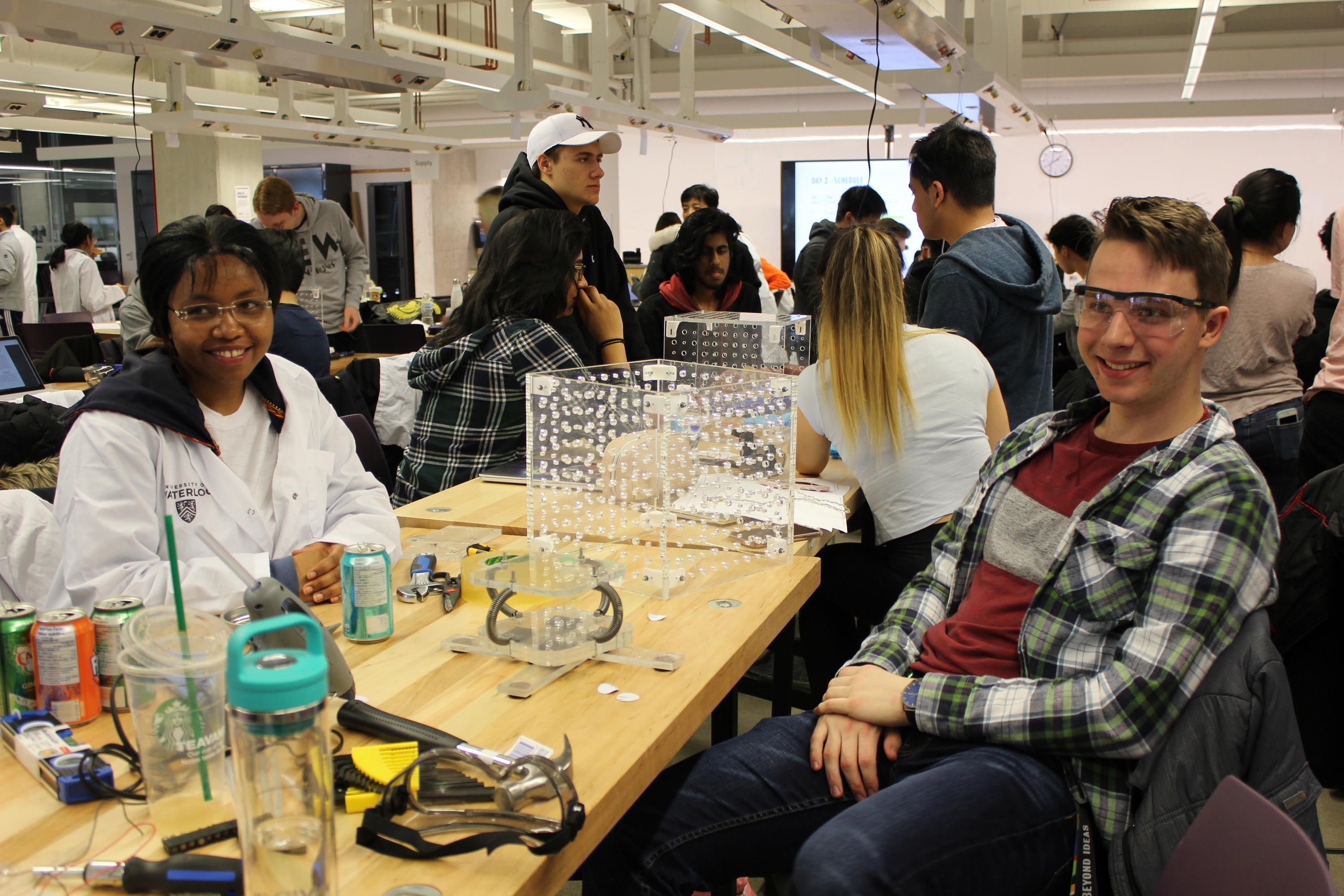
Ryan Li, a 1B student who participated, says “It was an amazing experience, and we got to learn so many new things. We hand-built each component, including an amplification circuit, a piezoelectric sensor system, a chemical wet etch tip for the STM tip, and a noise dampening system for the STM itself. For the wet etch, our group used Tungsten as the tip material and a base as the etching mechanism.”
This popular event will be repeated for the next cohort of NE students during the spring 2019 term.