Mike and Ophelia Lazaridis Quantum-Nano Centre
A state-of-the-art facility at the heart of Waterloo’s quantum ecosystem, home to the Institute for Quantum Computing (IQC) and the Quantum-Nano Fabrication and Characterization Facility (QNFCF), supporting interdisciplinary research and quantum device development.
Research Advancement Centers 1 and 2
A collaborative research hub offering academic, commercial, and innovation space, with infrastructure developed by TQT and Quantum Valley Investments (QVI) to support advanced quantum experimentation and prototyping.
Virtual Lab Tours
TQT is investing in a broad research infrastructure with a complete suite of tools for design, materials, fabrication, merology, and testing of quantum devices. View 360° virtual tours of TQT and QNFCF labs below.
Lab Equipment
Researchers and industry representatives are welcome to inquire about gaining lab access by completing the Get connected form.
|
Equipment |
Description |
Supplier |
Capability |
PI |
|---|---|---|---|---|
|
He-3 Cryostat with 12T Magnet 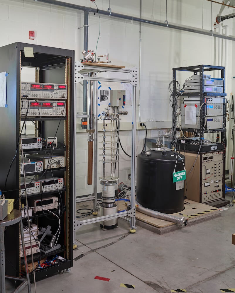 |
The He-3 Cryostat with 12T Magnet allows for materials characterization between 300mK and 300K. Rotation stages allow positioning of samples at any orientation to magnetic fields at low temperatures. 20 twisted pair DC lines and two microwave coaxial lines accommodate a wide range of electrical measurements. |
Janis Research Company | Testing / Characterization | George Nichols |
|
1.25 mW Leiden Dilution Refrigerator  |
A high-power, high-access ultra-low temperature platform for quantum information experiments. 1.4mW of cooling power at 100mK allows for multiple experiments and extensive cryogenic classical electronics. 20 microwave lines including three High Electron Mobility Transistor ultra-low noise preamplifiers provide drive, coupling control and readout for quantum processors. Superconducting and mu-metal shields provide zero magnetic field environments for superconducting devices. A compensated 1T solenoid allows experiments into hybrid superconducting/spin systems. A nitrogen pre-cool loop enables fast experiment turnaround. | Leiden Cryogenics | Testing/Characterization | George Nichols |
|
2652 Water Jet Table 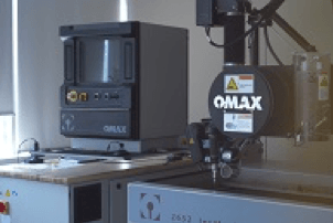 |
OMAX 2652 Water Jet Table with an X-Y cutting envelope of 4’4” x 2’2”. Allows for fast cutting of parts with high precision. It uses high-pressure water and natural garnet abrasive material to cut a variety of materials. It is able to provide precision parts based on 3D CAD models. |
OMAX | Coming soon. | Ivar Taminiau |
|
Cryostat with 20T Magnet (Kelvinox)  |
This system consists of a 20 T magnet and top-loading dilution cryostat enabling rapid electrical transport measurements in extreme high-field/low-temperature conditions. | Oxford Instruments | Coming soon. | George Nichols |
|
Diamond Growth System 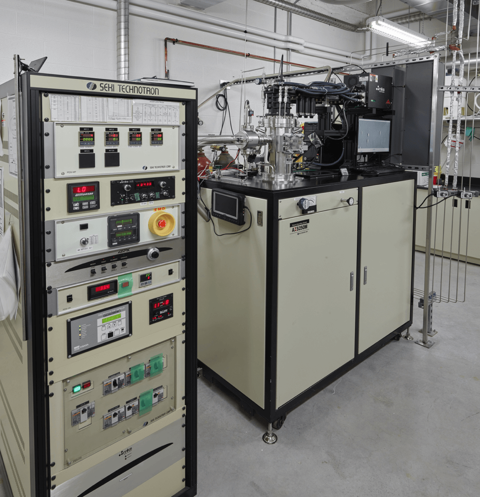 |
The Seki Diamond Growth system uses chemical vapour deposition techniques. The system can grow diamonds up to several microns in depth, with the option of adding nitrogen vacancy or phosphorus vacancy centres. Our Seki Diamond Growth System grows diamond layers for use in testing experiments. These diamond layers can be doped with impurities at the request of the researcher, with nitrogen vacancies, and phosphorous vacancies both available. Our Diamond Growth System uses ionized diamond components to grow diamond chips. We keep the system environment at high temperature (950° C to 1000° C), which allows the diamond growth mechanism to dominate. | SEKI Diamond Systems | Fabrication/Deposition | TBC |
|
Moore Nanotech Diamond Turning Machine 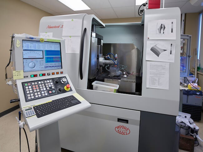 |
Our Moore Diamond Turning Machine provides a platform for ultra-high precision machining tasks. The design of the machine, as well as the vibration and temperature provide an extremely stable platform for machining, With this system, we are able to machine nanometer finishes and micrometer tolerances on a wide range of parts and materials like optical components, x-ray interferometric components, and neutron interferometric components. Used for machining of precision diamond optics. Can be tuned for nanometer finishes, and micrometer tolerances, for optical, x-ray, and neutron interferometric components. |
Moore Nanotech Systems | Preparation | Ivar Tamininiau |
|
60L/day He Liquefier 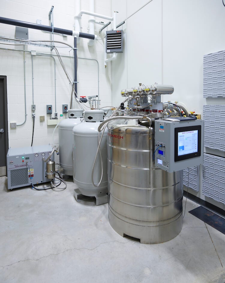 |
Helium Recovery System – A series of tubes that can be connected to Helium refrigerators to recover any leaked helium gas. These tubes feed into a refrigerator and compressor system that stores the helium for later use. RAC2 uses a building-wide Helium recovery system. This system recovers and recycles ~90% of all helium used in cryogenic experiments. Any experiments using Helium gas are hooked onto a recovery tube in the local lab. Helium gas recovered through this tube is collected and super-cooled again, before being stored for use in future experiments. We use this He recovery system to guarantee regular, reliable supplies of Helium for experiments. Our Helium recovery system is the largest of its type on campus. It has been in operation since 2016, and as of summer 2018, has recovered over 17,000 Litres of Helium. With this recovery system, we are guaranteeing regular supplies of valuable Helium for our researchers. |
Cryomech | Preparation | Don Carkner |
|
Thin Film Evaporation Sputter System  |
Provides thin films on chips using radio frequency (RF) and direct current (DC) sputtering methods, as well as molecular beam epitaxy (MBE). Able to grow most film substances on chips in high vacuum conditions. Our AJA Thin Film Growth system uses radio frequencies (RF) to sputter semi-conducting and insulating materials on chips. The AJA system also deposits layers of conductors on chips using direct current (DC) sputtering. Both RF and DC methods are examples of sputtering methods to make amorphous, thicker layers. In addition to sputtering, our AJA system is capable of using molecular beam epitaxy (MBE), to grow multiple thin layers of materials. Sandwiched layers grown using MBE are made for research into topics like modern semi-conduction and semi-conducting chips. Our AJA Thin Film Growth System is capable of growing oxides, alloys, pure metals, and more on chip substrates made of substances including sapphire, silicon, quartz, fused silica, and others. |
AJA International Inc. | Fabrication/Deposition | TBC |
|
Micro Manipulated Probe Station ST-2.6T (Low Temperature Probe) 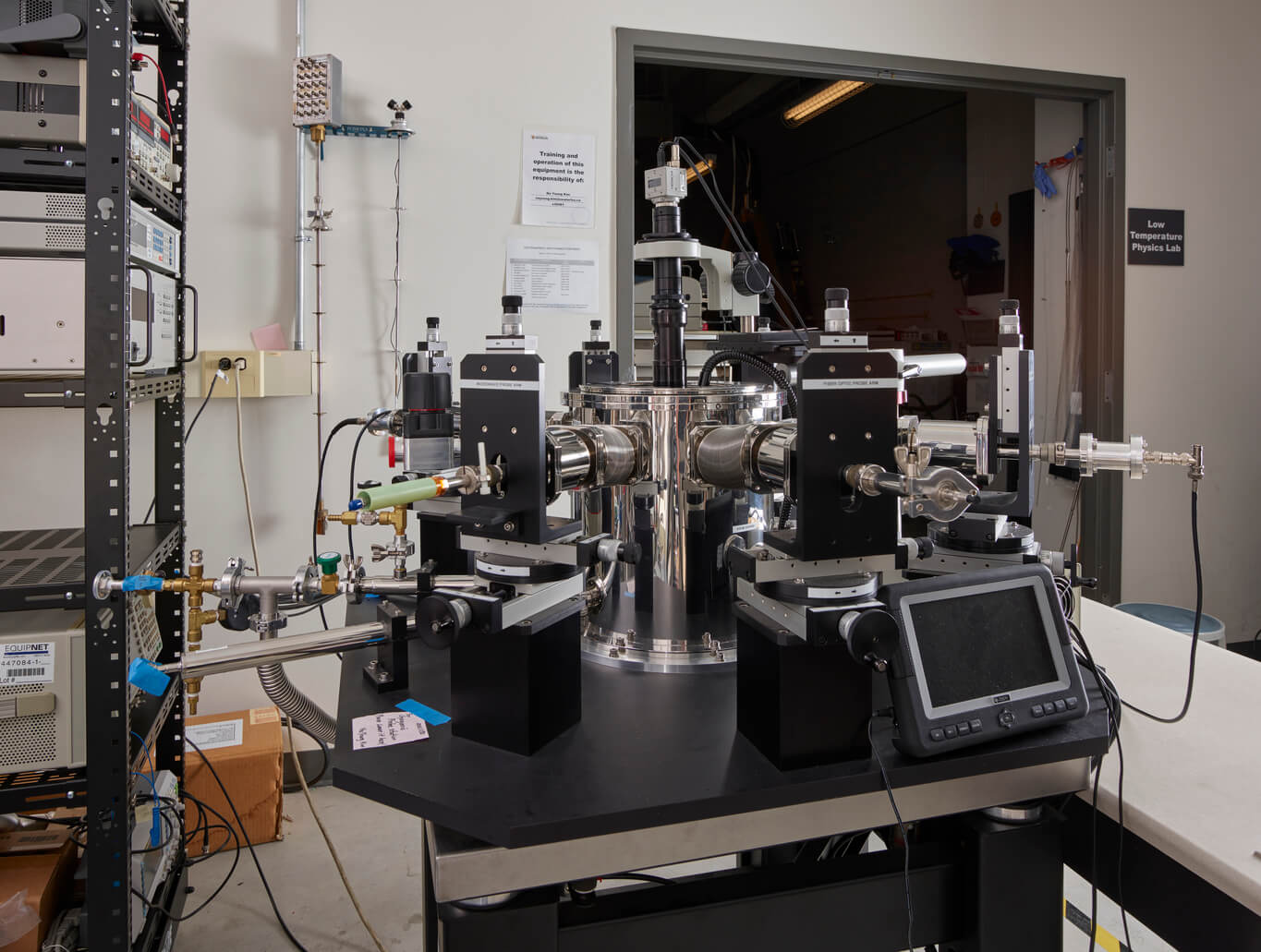 |
The Janis Research Model ST-500 is a continuous-flow cryogenic probe station designed for DC, low-frequency, and high-frequency measurements, with microwave (MW) and fiber-optic capabilities. It operates over a wide temperature range from approximately 5 K to 400 K. This tabletop system is also equipped with a magnet, providing a maximum magnetic field at the sample mount up to 2.6 T at 5 K. The system operates in continuous flow mode using liquid helium. | Janis Research Company | Transport | Na Young Kim |
|
Si-Nanowire System 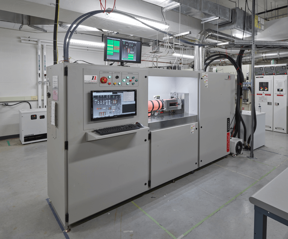 |
The FirstNano CVD system is an automated, precision 3-zone furnace designed for the growth of silicon nanowires. It enables the synthesis of single-crystal Si nanowires with growth parameters controlled through programmable recipes and catalyst configuration. The system supports Vapor–Liquid–Solid growth (VLS), in which a transition metal catalyst forms a liquid eutectic alloy with silicon at elevated temperatures. A silicon precursor gas, such as silane (SiH₄), thermally decomposes to release silicon atoms, which dissolve into the liquid catalyst droplet. Upon reaching supersaturation, silicon precipitates at the liquid–solid interface, resulting in the axial growth of a nanowire beneath the catalyst droplet, which is lifted as growth proceeds. The system is equipped with a gas delivery system for HCl, SiH₄, H₂, He, and N₂, along with variable vacuum control and an integrated hazardous gas abatement system. |
Firstnano, CVD Equipment Corporation | Fabrication/Deposition | Taso Alkiviades |
|
Bruker EMX X-band ESR 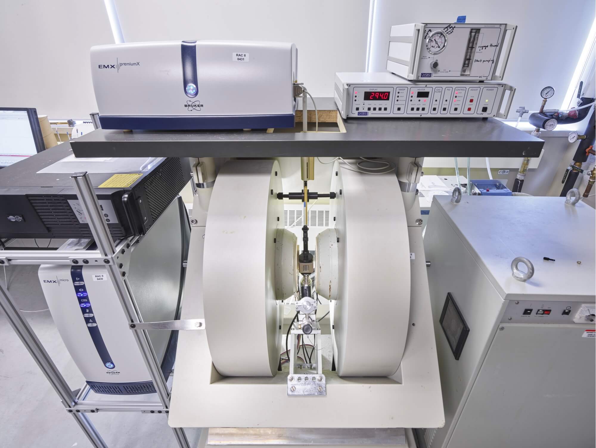 |
Consists of a large electromagnet pair that generates a consistent field across the sample space, an X-band microwave source, and a liquid helium cryostat capable of holding samples at room temperature down to cryogenic temperature. This system is used for electron spin resonance (ESR) and radical electron sensing. Both our pulsed and continuous wave systems are equipped with liquid helium cryostats, allowing us to perform experiments at cryogenic temperature. Electron spin resonance (ESR) is used to study the couplings between electrons and nuclear spins. Continuous wave ESR (CW-ESR) is performed under continuous microwave bombardment from a nearby source. CW-ESR can be used to study electron nuclear double resonance (ENDOR). The microwave frequencies used in experiments can be tuned to match the Zeeman energy gap in a two level system. |
Bruker BioSpin Ltd. |
Characterization | Fatemeh Fani Sani |
|
Low Temperature (4K) Scanning-Tunneling Microscope with Q+ AFM ![Low temperature scanning tunneling microscope [Omicron-LT-STM]](/transformative-quantum-technologies/sites/default/files/uploads/images/omicron-stm-with-afm.jpg) |
Omicron STM with AFM – Provides high resolution atomic images of conductive, semi-conductive, and insulator samples in high-vacuum atmospheres using STM and AFM techniques. Capable of holding Helium temperatures for 50+ hours, and Nitrogen temperatures for up to a week. Our Omicron STM with AFM performs topography measurements of samples in a high vacuum, cryogenic temperature system. These cryogenic temperatures are achieved using helium and nitrogen bath techniques. Helium bath cryogenics achieve temperatures of 4.7 K, and can be kept at temperature for 50+ hours. Nitrogen bath Cryogenics achieve temperatures of 77K and can be kept at temperature of up to a week. Our STM with AFM system is magnetic field capable. Using this field, we are able to perform measurement experiments on polarized spins. Our STM with AFM can image single atoms (as opposed to NMR which is only able to image thousands at once). |
Scienta Omnicron | Characterization | Sandra Gibson |
|
Small tube furnace 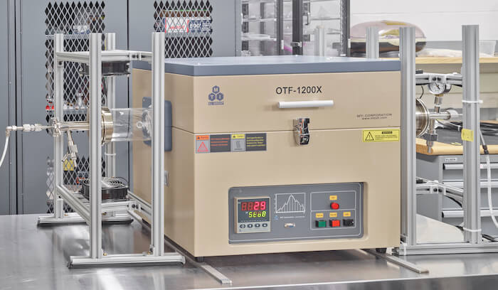 |
One zone furnace with capable of reaching 1200ºC. Able to conduct experiments with different internal environments (Oxygen, Argon, Hydrogen). |
MTI Corporation | Testing/Characterization | TBC |
|
D8 Venture X-Ray Diffraction 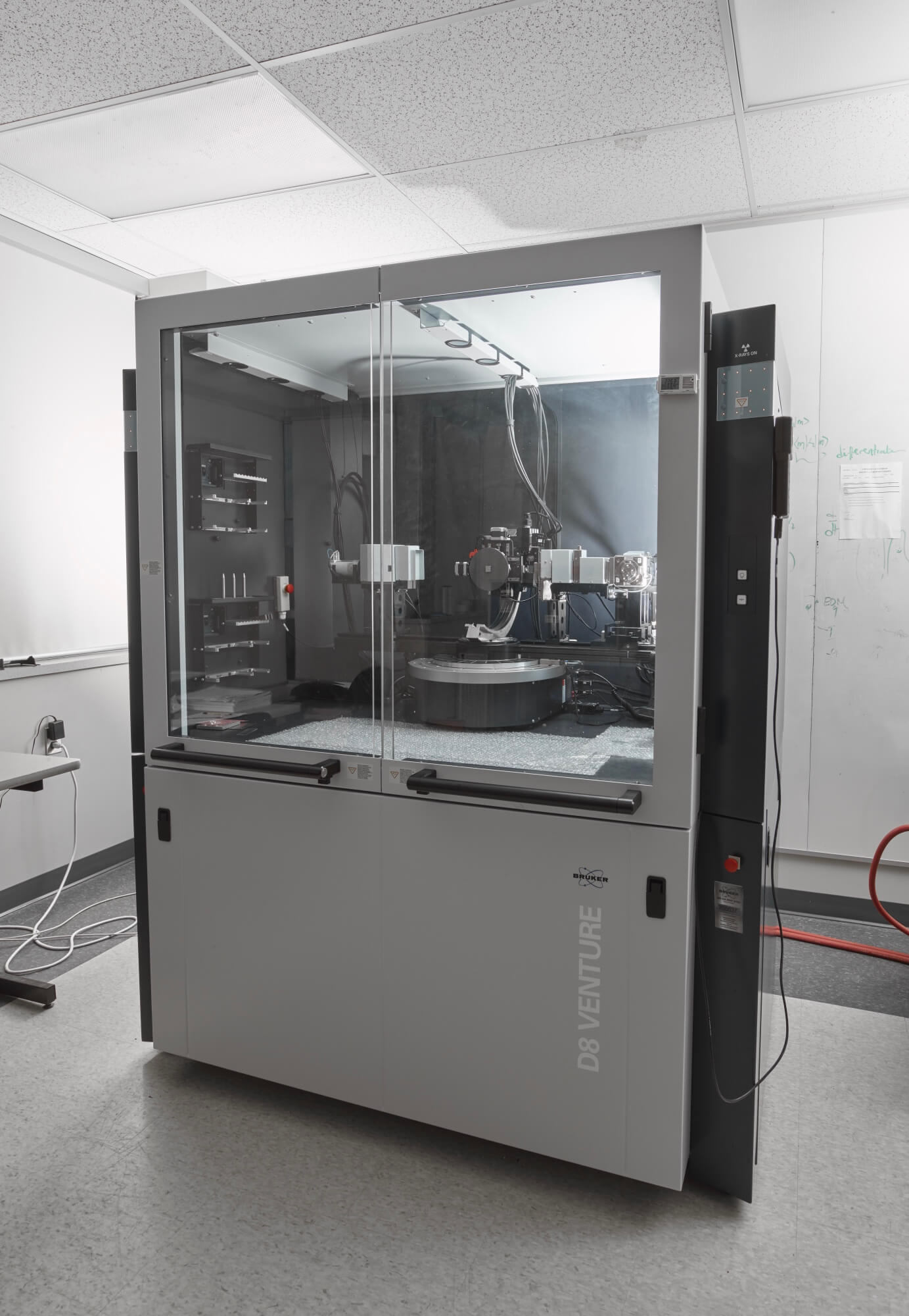 |
An experimental setup with photon detector, X-Ray sources, anode sources. Capable of Cu-radiation, Mo-radiation, and Ag-radiation. | Bruker BioSpin Ltd. | Characterization | Sandra Gibson |