What has been done
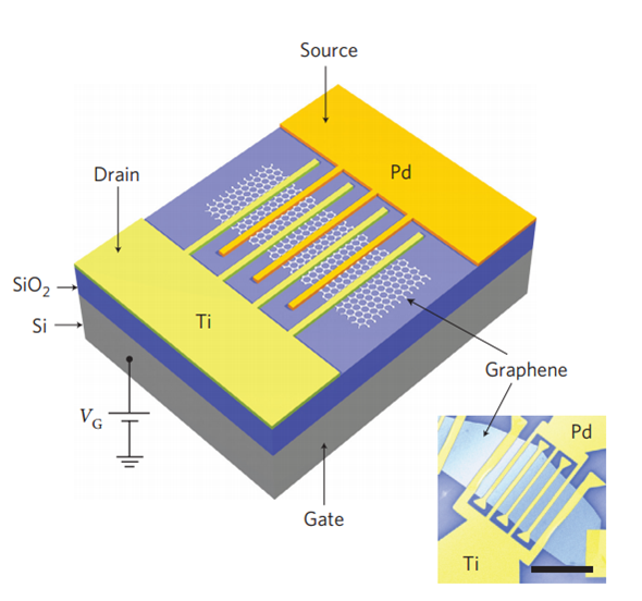
- Developed graphene-based nano device templates for transistor, bio-sensor and photo-detector applications; and started packaging and integrating them into CMOS systems.
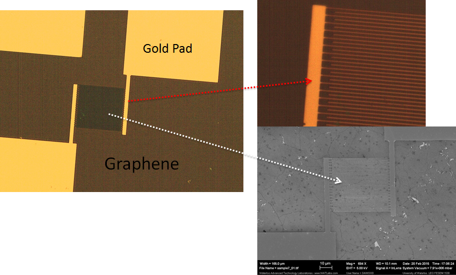
- Successfully etched graphene films of 100 mm in thickness using reactive ion etching (RIE) for the first time (to our knowledge).
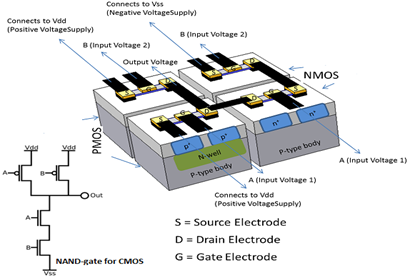
- Started modelling of nano-chips on CMOS systems design using COMSOL Multiphysics, and are investigating the required high level circuits.
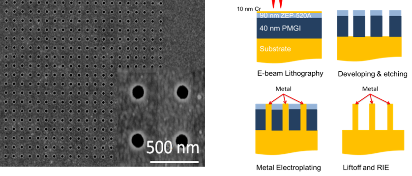
SEM image of nanohole machining using electron beam lithography (EBL) and developed lift off process
Schematic diagram of nanowire (NW) fabrication using electron beam lithography and electroplating
From bottom to top:
-Silicon wafer -Graphene, monolayer -MoS2, monolayer -Gold film, 150 nm -Copper wire, 90 nm
-Graphene, 40 nm -MoS2, 15 nm
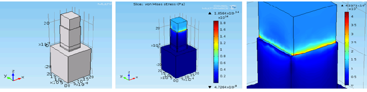
-Stress at pad/wire interface
Sensor using graphene gel as a channel between two electrodes
Summary
-
Substantial challenges involve in testing and packaging the nano chips and integrating them into micro systems (MEMS), including fabrication, higher contact resistance and interlayer residual stresses.
-
Graphene can address some of these challenges as potential interconnector to achieve low contact resistance for fast electronics.