2D TMDs an emerging family of layered materials, have provided a fertile ground for harvesting fundamental science emergent applications.
TMDs can contain a number of different properties and structural defect which significantly alter their physco-chemical properties. TMDMs exhibit diverse electronic properties, ranging from insulation hexagonal boron nitride and semiconducting transition metal dichalcogenides such as molybdenum disulphide, to semimetallic graphene. 2D materials exhibit many exceptional properties. First, quantum confinement in the direction perpendicular to the 2D plane leads to novel electronic and optical properties that are distinctively different from their bulk parental materials. Second, their surfaces are naturally passivated without any dangling bonds, which makes it easy to integrate 2D materials with photonic structures such as waveguides and cavities [1].
Engineering of different TMDMs with tunable electrical and optical properties are a key approach to controlling the transport characteristics of future electronic and optoelectronic devices. For example, modern electronics require channel materials to be ultra-thin, and therefore 2D materials are coming into key. Semiconductor transition metal dichalcogenide materials in common form of MX2(M:Mo, W and X=S,Se), exhibit numerous fascinating properties associated with their reduced thickness [2].
Integrating TMDMs sheets and nanoparticles with sensors brings unique optical properties, excellent electrical conductivity, large surface-to-area ratio and high sensitivity and resolution power in a single nano/micro chip.The large surface area of 2D materials enhance the surface loading of desired molecules and their excellent electrical conductivity can be beneficial for conducting electrons between molecules and electrodes.
Optical and plasmonics properties of these materials could enhance the surface plasmon and luminescence properties of detectors and increase the sensitivity and the resolution of the transmitted or reflected wavelengths in an optical bio/chemical sensor.
TMDMs will enables sensors that smaller and lighter, providing endless design possibilities. They will also enable to detect small changes in matter, work more quickly and less expensive than traditional sensors.
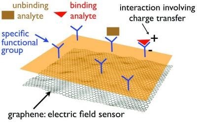
A schematics diagram of detecting bio-molecules based on the charge transfer in a FET graphene sensors[3].
[1]. Fenginan Xia et.al., Nature photonic, 2014,8, 899–907
[2]. Zhong Lin et al. 2D Materials, 2016, 3, 022002
[3]. www.graphene-info.com/graphene-sensors