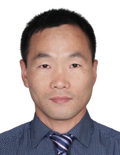
His current research fields are nanofabrication processes (e-beam lithography, deep RIE) and nanodevice manufacturing. He has been working on nanofabrication of metalens, augmented reality gratings and waveguide sensors with collaborators in the U.S., Canada, etc. He has developed 17 years of expertise in micro- and nanofabrication techniques, such as e-beam lithography, x-ray lithography, photolithography, cryogenic and room-temperature Si deep reactive ion etching, electrochemical deposition, and material/nanostructure characterization methods including SEM, EDX, XPS, XRD, TEM, TKD, etc. So far, he has published 93 articles and has been granted 23 patents. These works have been cited a total of 1400 times.
