Background
Microelectronic wire bonding is a process used to interconnect integrated circuits (ICs) on microchips to substrates or boards. Wire bonds provide electrical signals and power for the IC. The most common process to attach the wires to the metallized surfaces is using ultrasound as a bonding agent. Minimizing cost and size while maximizing quality are the goals. By improving microjoining of the internal wires in devices, the size of devices can go down and costs can be reduced.
Research areas - New materials
Cu bonding wires
Insulated bonding wires
Ni based metallizations
Research with all these new materials is underway, addressing issues and roadblocks that currently slow down the introduction of these materials together with their expected benefits.
Research areas - Low-stress bonding
The focus is on enabling low-stress ball bonding using Cu and insulated wires. The goal is to find ways to reduce the mechanical forces and stresses required to form acceptable bonds. Some objectives of the research are: (i) to investigate the effect of various input parameters on the physical mechanisms underlying the process process, and (ii) to analyze the failure criteria for underpad damage and correlate it with the process mechanism.
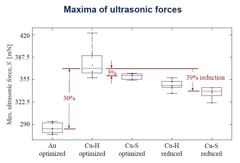
Comparison of maximum ultrasonic force measured by the microsensor for five different processes [Shah et al, Proc. of 58th ECTC, 2008 (PDF)]
Mechanisms of bonding and failure
The focus is on understanding the bonding and failure mechanisms of different wire bond processes such as Au/Al process, Cu/Al process, Al/Al process. Specific topics of interest include: (i) long-term reliability tests (ii) in situ process monitoring using microsensors and (iii) theoretical modeling and finite element simulation.

Facilities
Wire bonding
- Automatic Wire Bonders: ESEC 3100, ESEC 3088
- Manual Wire Bonders: K&S 4524D, K&S 4523AD
Mechanical testing
- DAGE 4000 Tester for wire bond shear and pull testing

Non-destructive gold wire pull-test

Footprint of a sheared copper ball bond
- Instron 5548 Micro Tester for tensile testing of bonding wire
- Hardness testing using microhardness tester and nano-indentor

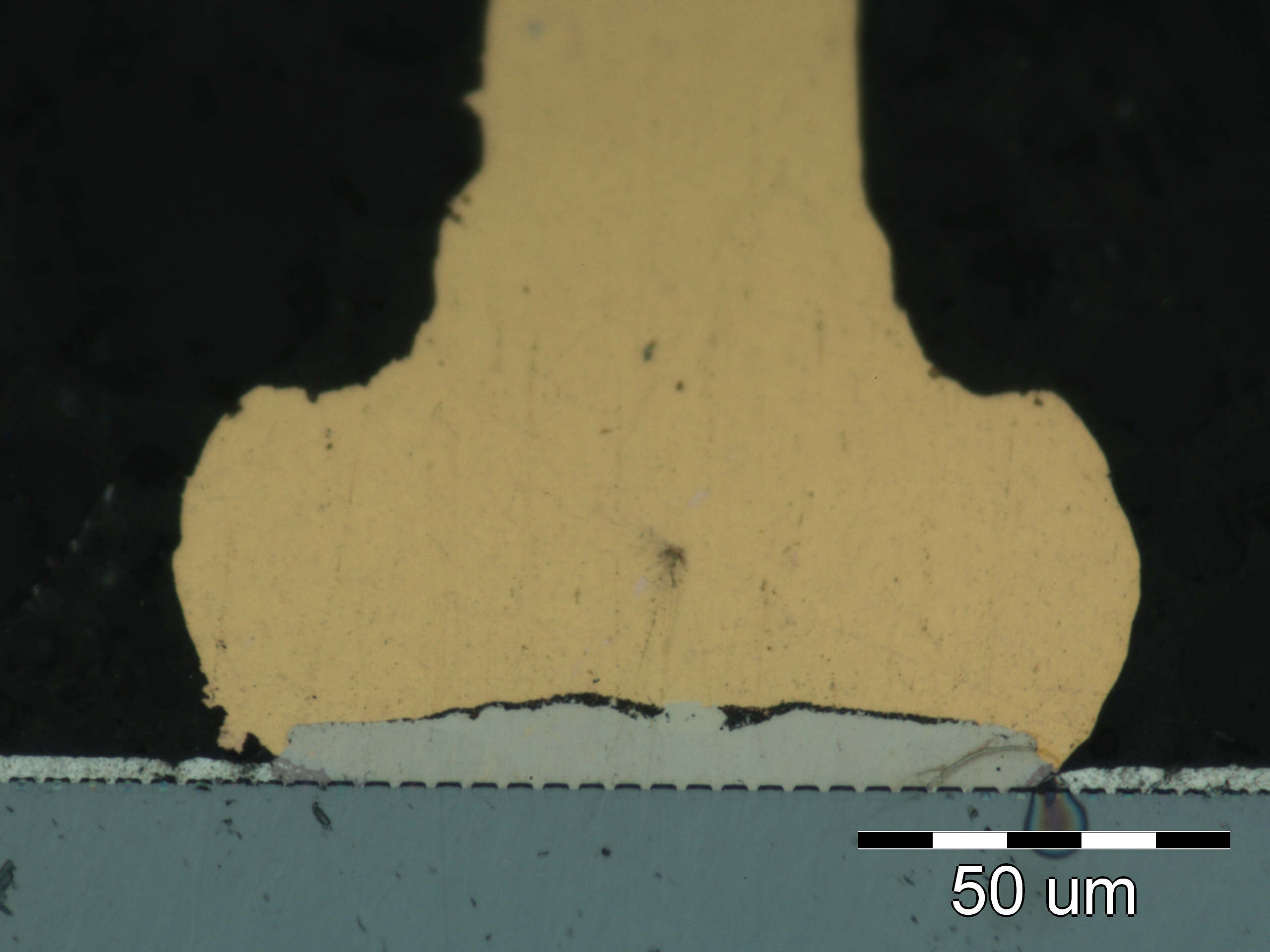
Cross-section of a Cu ball bond with Vickers microhardness indentation mark [Pequegnat et al, J. of Mat.: Mat. in Elec., 2009 (PDF)]

Cross-section of a Au free air ball with Vickers nanohardness indentation marks
Modeling and simulation
- State of the art computing facilities with access to commercial simulation software such as COMSOL, ABAQUS, ANSYS
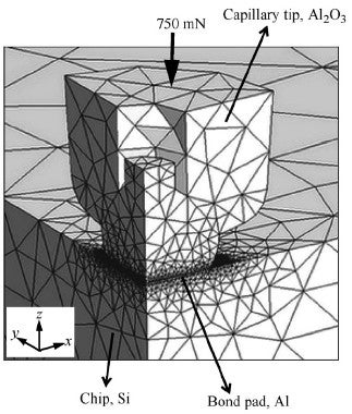
FE plane stress-strain model of ball bonding using COMSOL 3.3 [Shah et al, Sensors and Actuators A148(2), 2008 (PDF)]
Microsensors
- Low-stress bonding and chip damage studies
- Long-term reliability studies
- Bonding and failure mechanism studies


Sample preparation
- Mechanical polishing
- Ion milling: low angle ion milling and polishing system Model 1010, Fischione Instruments
- Chemical etching: for underpad silicon damage analysis
Microscopy
- Optical microscopes
- Scanning electron microscopes (SEM)
- Environmental scanning electron microscope