Micro-electromechanical systems (MEMS) reliability

Fabrication reliability

Fabrication of free-standing MEMS is fraught with obstacles. Residual stresses which present themselves during various phases of the depositions, and etching processes can have severe effects on the performance of MEMS devices. Internal mechanical stresses cause the free-standing microstructures to warp, buckle up, bent down and ultimately touch down onto the supporting substrate, thus deteriorating the performance of the microsystem or even causing complete failure (Cianci, Coppa, and Foglietti, 2007). In addition, the multilayer nature of most MEMS devices causes additional residual stress to present itself because of the variations in material properties between two layers; the inconsistencies in thermal expansion between layers exacerbates the residual stress issues. Attempts to control residual stress using different fabrication techniques are being implemented, and have been successful in reducing the negative effects of stress. However, development of optical microstructures such as microbolometers needs nanometer scale control of thin-film shape, thus greater control of residual stresses (Bifano, Johnson, Bierden, and Mali, 2002). Hence, a suitably accurate and efficient method for residual stress measurement is required.

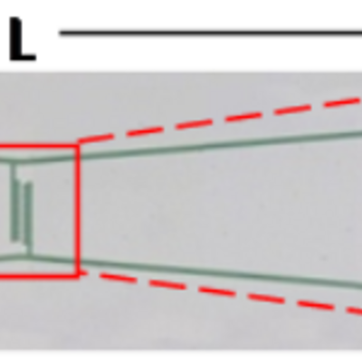
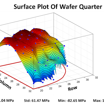
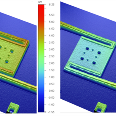
The Sensors and Integrated Microsystems lab (SIMSLab) is currently focusing on a method for the reliable characterization of residual stress caused by fabrication. In-situ stress measurement devices (Fig. 1) are being used to extract accurate values of residual stress. Since MEMS are fabricated using a wafer deposition process, the use of in-situ devices allows us to gather localized measurements of stress over the entire surface of the wafer (Fig. 2 and 3). Knowing the local residual stress trends in a wafer, we are able to identify wafer sites which minimize residual stress effects, allowing designers to increase the fabrication yield of their devices.

Therma-opto-electro-performance modeling

A key determining factor in the reliability and lifetime of uncooled microbolometers is their on-device temperature distribution. For instance, the distribution of heat in the microbolometer structure governs the thermal stress, and hence the deflection experienced by it. Variation in temperature of the surface of the microbolometer can affect its ability to accurately measure incoming radiation. Accurate knowledge of these deflections is required in order to predict various performance and failure modes for the device. Therefore, knowledge of the temperature distribution is critical (Nieva, Godin, Effa, Bidaux, McIsaac, and Pope, 2010).

At SIMSLab thermal-opto-electro-mechanical modeling of the microbolometer is being done using both finite difference and finite element methods (Fig. 4). The goal of this research is to produce a model which will accurately predict the performance and lifetime reliability of microbolometers. Justification of modeling is being researched using fabricated test devices (Fig. 5).

Characterization of mechanical properties

Information on material properties of structural thin films for MEMS fabrication is rather limited. However, the mechanical properties of the film greatly influence the device operation. At times, this dichotomy leads to a properly designed device failing or not meeting the expected results produced by a model. This, in turn, creates a lot of unnecessary issues for the researchers which at best wastes time and at worst causes the abandonment of a good idea.

The goal of this project is to create a suite of on-chip devices that can be used the measure the material properties of the thin film and ascertain that they are as expected. Currently, two specialized projects are underway.

The first focuses on measuring the change in the mechanical properties of polycrystalline and single crystalline silicon with varying levels of phosphorus doping. Phosphorus is often used to reduce the residual stress in polysilicon, however the other effects of the phosphorus doping are often neglected. Once this project is complete the results can be extrapolated to predict the effects of other common silicon dopants.

The second project focuses on characterizing the mechanical properties of silicon nitride. This poses special challenges as silicon nitride is an insulator and the mechanical properties vary widely with the deposition technique.

Current project members