Neil Sarkar has given new meaning to the expression “put under the microscope.”
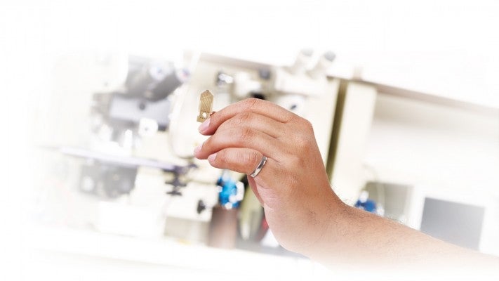
The electrical engineering post-doctoral researcher has developed the world’s first single-chip atomic force microscope (AFM) that opens up a world of possibilities for research and development in industries ranging from electronics to bioscience.
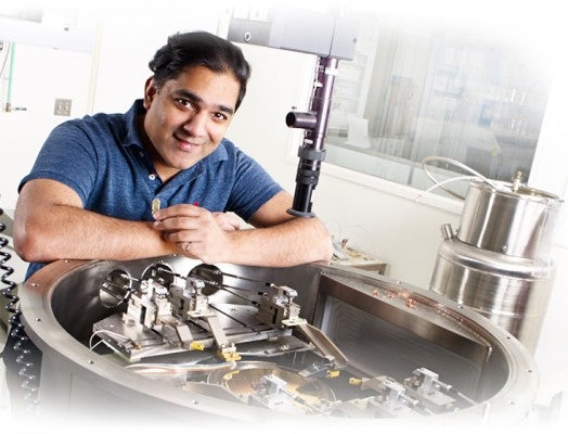
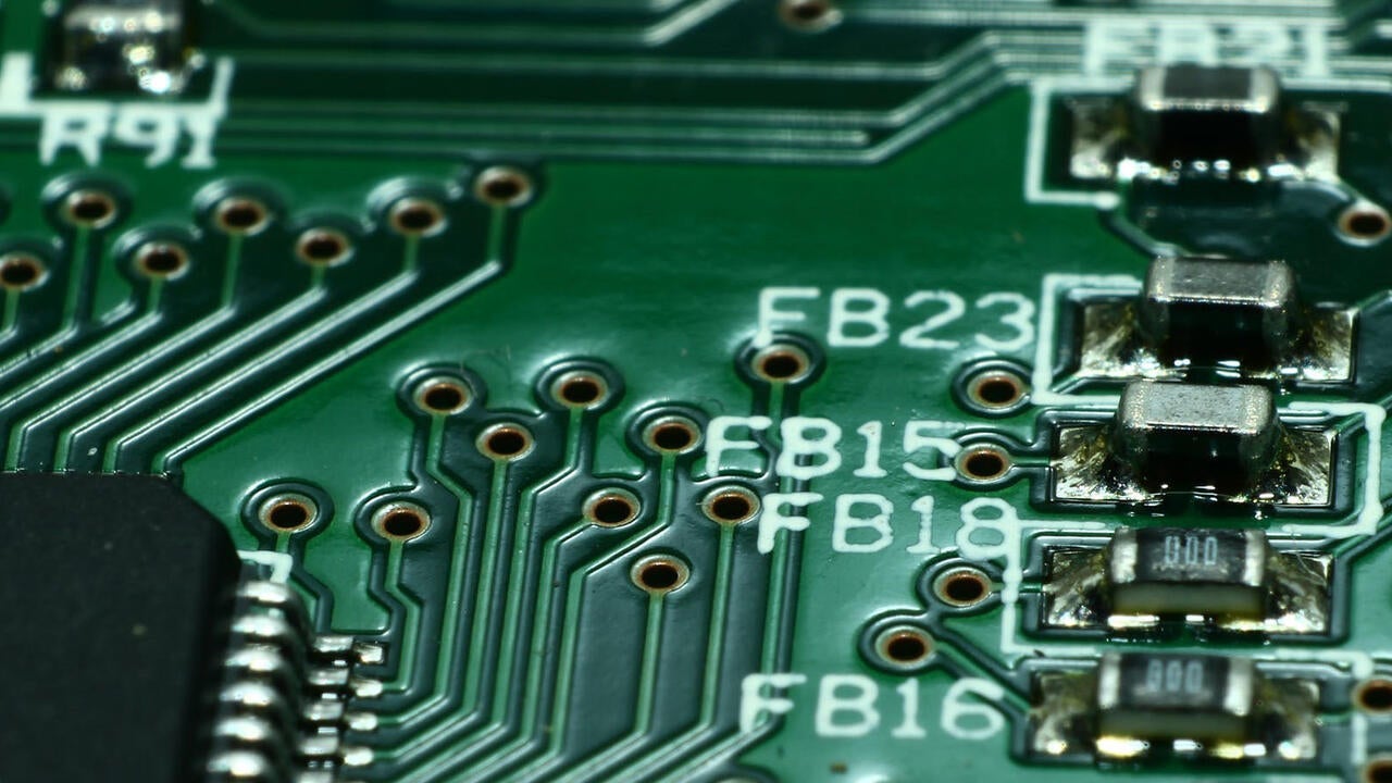
Barely visible to the naked eye, Sarkar’s $1,000 microscope combines all the components of current AFM technology on a silicon CMOS-MEMS chip that operates at a mere fraction of the size and price of traditional high resolution microscopes costing up to $100,000. And companies could benefit from other substantial savings gained from being able to more quickly and accurately observe flaws and faults only visible at the nanometer scale.
“We’re really close to outperforming the types of instruments that people have in their labs today,” says Sarkar.
Last year, the Waterloo electrical engineering graduate and member of the Centre for Integrated RF Engineering was presented with CMC Microsystems’ Douglas R. Colton Medal for his work that has also been recognized with two Manning Awards for Canadian Innovation.
Sarkar, who used a fibre optic microscope for a high school science fair project, says he’s always been interested in microscopy. But his future in the field became more focused at Zyvex Labs, an American nanotechnology company, where he spent his last two undergraduate co-op terms and was eventually hired on full time.
“It was there that I came up with the idea for a nanoscale microscope that everyone could eventually have access to,” Sarkar recalls.
Startup launched to commercialize technology
Eight years ago Sarkar left his job and returned to Waterloo Engineering to pursue his PhD in electrical engineering. He was enticed by the opportunity to work with Raafat Mansour, the Canada Research Chair in Micro and Nano Integrated FR Systems, and by the University’s IP policy, which provides researchers with intellectual property rights to anything they discover. At the same time, he and Mansour launched Integrated Circuit Scanning Probe Instruments (ICSPI) where Sarkar’s technology is now being commercialized.
The company has been preselected to deliver 40 of its AFMs to the federal government’s Build in Canada Innovation program and soon its technology may be included in several college curriculums. Sarkar’s goal is to have his microscope used more widely in high school classrooms, but admits cost may be a deterrent to educational institutions already strapped for cash.
“We may have to find some benefactors who want to improve the quality of education and allow students to see things they’ve never seen before,” he says.
Future plans include using the technology to improve just about anything from medical instrumentation to camera phone lenses and 3D printing.
Sarkar credits Waterloo Engineering for the drive to succeed in his field.
“As an undergraduate student I was lucky to be in a classroom with others who were as enthusiastic as I was about being an engineer,” he says. “There’s a culture on campus of wanting to be the best and accomplishing things that are out of the ordinary scope of engineering.”