Vendor: JEOL [JEOL press release: May 6, 2015]
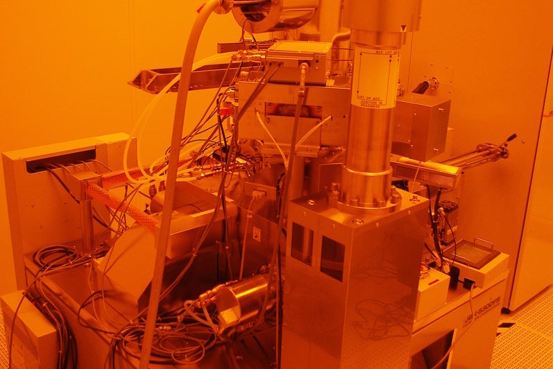
Model: JBX-6300FS electron beam lithography system
Purpose: Patterning nanometer scale features via electron-beam lithography
Equipment description:
The JBX 6300FS features a Schottky thermal field-emission (TFE) electron source with a 100 kV accelerating voltage, to achieve extermely stable high resolution patterning. With multiple beam currents and two writing modes to choose from, users can write small features precisely and large features quickly. The tool software offers numerous automated calibration routines allowing the tool to be calibrated consistently, and continuously calibrated during long exposures to counteract any small fluctuations. Users of this tool are giving access to the BEAMER sofware package for preparing files, and implementing a number of process corrections such as proximity effect correction.
System features and options:
- Gaussian beam lithography system employing TFE gun & vector Scan method
- 100 kV accelerating voltage
- 50 MHz pattern generator with a 19 bit DAC
- Stage positional step size of 0.125 nm (high resolution mode) or 1 nm (high speed mode)
- Field size: 0.5 mm x 0.5 mm (high speed mode) or 62.5 μm x 62.5 μm (high resolution mode)
- Available apertures: 300 μm, 130 μm, 90 μm, 60 μm, 40 μm, 25 μm with automated selection via software control
- Stitching performance: ≤±9 nm (high resolution) or ≤±20 nm (high speed)
- Overlay accuracy: ≤±9 nm (high resolution) or ≤±20 nm (high speed)
- Measured minimum beam spot size: ≤2.9 nm
- Access to GenIsys BEAMER, TRACER and Juspertor Layout Editor software packages


