Background
Advances in electron microscopy resolution have enabled gaining insight into reaction dynamics at an atomic level for solid samples. Extending this capability to in-situ imaging of liquid systems would further enable discovering the full range of atomic motions and behaviors in such areas as protein folding, nucleation growth and self assembly.
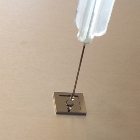
Commercially available Nanofluidic Chip (NFC) systems for in-situ liquid imaging are generally comprised of two Silicon wafer based nanofabricated chips with transparent windows separated by a thin spacer (typically in the order of a few hundreds of nm). However, even a tiny droplet of 0.1 uL overflow of the windows spacer increases the effective electron beam path in a non-reproducible manner.
The main problem with current NFC systems is the inability to accurately and precisely control of the final liquid layer thickness and the positioning of the liquid sample (droplet).
Description of the invention
A new universal NFC and loading station system have been developed that avoids this problem entirely by providing a reservoir area (or overflow catch basin) to capture the excess fluid and drain it away from the spacer thereby leaving the viewing area unaffected.
Advantages
University of Waterloo (UW) NFCs allow for the excess of liquid to spill over into an adjacent reservoir, without reaching the spacer area. In addition, the special shape of the chips enables the liquid droplet to self-position in the viewing area and pre-concentrate at desired level before sealing. This NFC is loaded in a specially designed loading station for minimal to no window bulging to enable control of the effective electron beam path or liquid layer thickness, and therefore better resolution images of drop-casted specimens over large viewing areas. Moreover, this NFC have been fabricated to fit in most commonly used sample holders.
Potential applications
Our innovative new universal NFC system will enable:
- In-liquid electron microscopy imaging of nanomaterials and biospecimens.
- Observation of dynamical processes such as chemical reactions, self-assembly processes, etc. with sub-nanometer resolution.
- Electron microscopy studies of pre-fixed specimens onto the inner surface of the window such as cells, viruses, nanoparticles and more.
- Electron tomography studies of in-liquid specimens.
Reference
10153 & 10205
Inventor(s)
Dr. German Sciaini
Dr. Ariel Petruk
Patent status
Patent applicaton filed
Stage of development
Prototype
Contact
Scott Inwood
Director of Commercialization
Waterloo Commercialization Office
519-888-4567, ext. 33728
sinwood@uwaterloo.ca
uwaterloo.ca/research