Background
There has been growing interest in a variety of 2D materials such as graphene, graphene oxide, hexagonal boron nitride, transition metal dichalcognides such as molybdenum disulfide, and more recently silicine and phosphorene. These materials have a range of unique properties and form a complete set of electronic materials which include conductors, semiconductors (direct and indirect band gap) and insulators which can, in principle, be arranged in various ways to build advanced electronic and optoelectronic circuits. Furthermore, single layers of these materials can be used as transparent conductors, blocking layers for food packaging or corrosion protection, or as selective membranes. The use of 2D nanomaterials in these applications requires the development of processing methods to deposit uniform thin films over large area and with fine control over film thickness or layer number.
Description of the invention
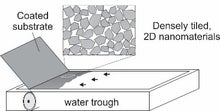
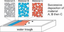
The invention is a method to assemble densely tiled monolayers of various 2D nanomaterials into large area films by edge-to-edge aggregation at the air-water interface. It enables the continuous deposition of one or more materials onto arbitrary substrates using roll-to-roll processing strategies. The invention also describes a method to pattern films to create electronic or optoelectronic circuits within a single monolayer which can also be transferred continuously.
Advantages
The film forming method described is economically attractive as it involves only a simple water bath and can be carried out under ambient conditions. This is in contrast to conventional approaches which require high vacuum conditions, expensive capital equipment and select high purity substrates. Our approach also offers the unique ability to pattern 2D materials with different electronic properties into one monolayer. It is ideally suited to create inexpensive coatings, membranes and electronic/optoelectronic components which can be transparent and flexible.
Potential applications
The method describes can be used to create films from a single material, can be patterned with multiple materials or can be coated multiple times to create thicker films of one or more 2D materials. These have a wide range of applications. Some of the most promising are listed below:
- Transparent barrier layers in food packaging
- Corrosion prevention
- Filtration membranes (pervaporation, ultrafiltration, reverse osmosis)
- Transparent conductors
- Flexible electronics and optoelectronic components
- Solar cells
Reference
7412
Inventor(s)
Michael A. Pope
Luzhu Xu
Yefeng Zhang
Patent status
PCT patent application filed
Stage of development
Process verified experimentally
Contact
Scott Inwood
Director of Commercialization
Waterloo Commercialization Office
519-888-4567, ext. 43728
sinwood@uwaterloo.ca
uwaterloo.ca/research