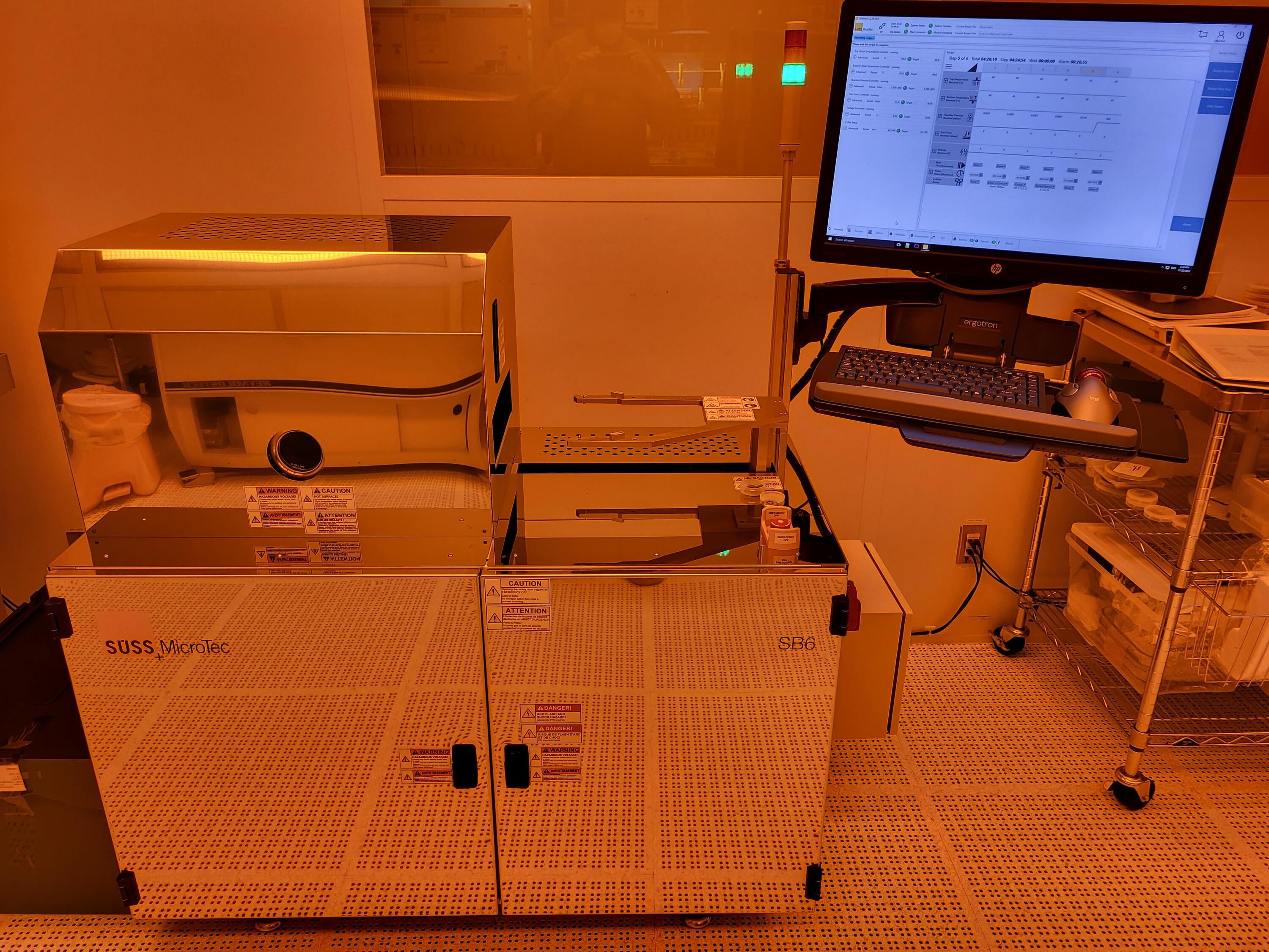
The SB6 wafer bonder from SÜSS Microtech is a semi-automated wafer bonder capable of executing a variety of different wafer bonding processes such direct and anodic bondings. The SB6 system may be used with the SÜSS BA6 aligner to enable alignment of substrates prior to the bonding process. The system is equipped with bonding fixtures enabling bonding of 100 mm wafers, 3″ wafers and smaller substrates.
The system features:
- 20 kN maximum tool force
- Turbopumped process chamber (achievable pressure < 5x10⁻⁵ mbar)
- 150 mm bond head with maximum temperature of 550℃
- Closed fixture
- Anodic bonding power supply up to 2000 V
-
Compatible
substrate
tooling
(bonder):
- 100 mm wafers
- 3″ wafers and small pieces
-
Bond
chucks
available
for
pre-bond
alignment
on
SÜSS
BA6
aligner:
- 100 mm wafers
- 3″ wafers and small pieces
This tool enables new process capabilities:
For more information about technical capabilities of the SÜSS Microtech SB6 and BA6, please contact Lino Eugene. Ken Speirs is the designated trainer for these tools.
Preliminary results for standard bonding techniques
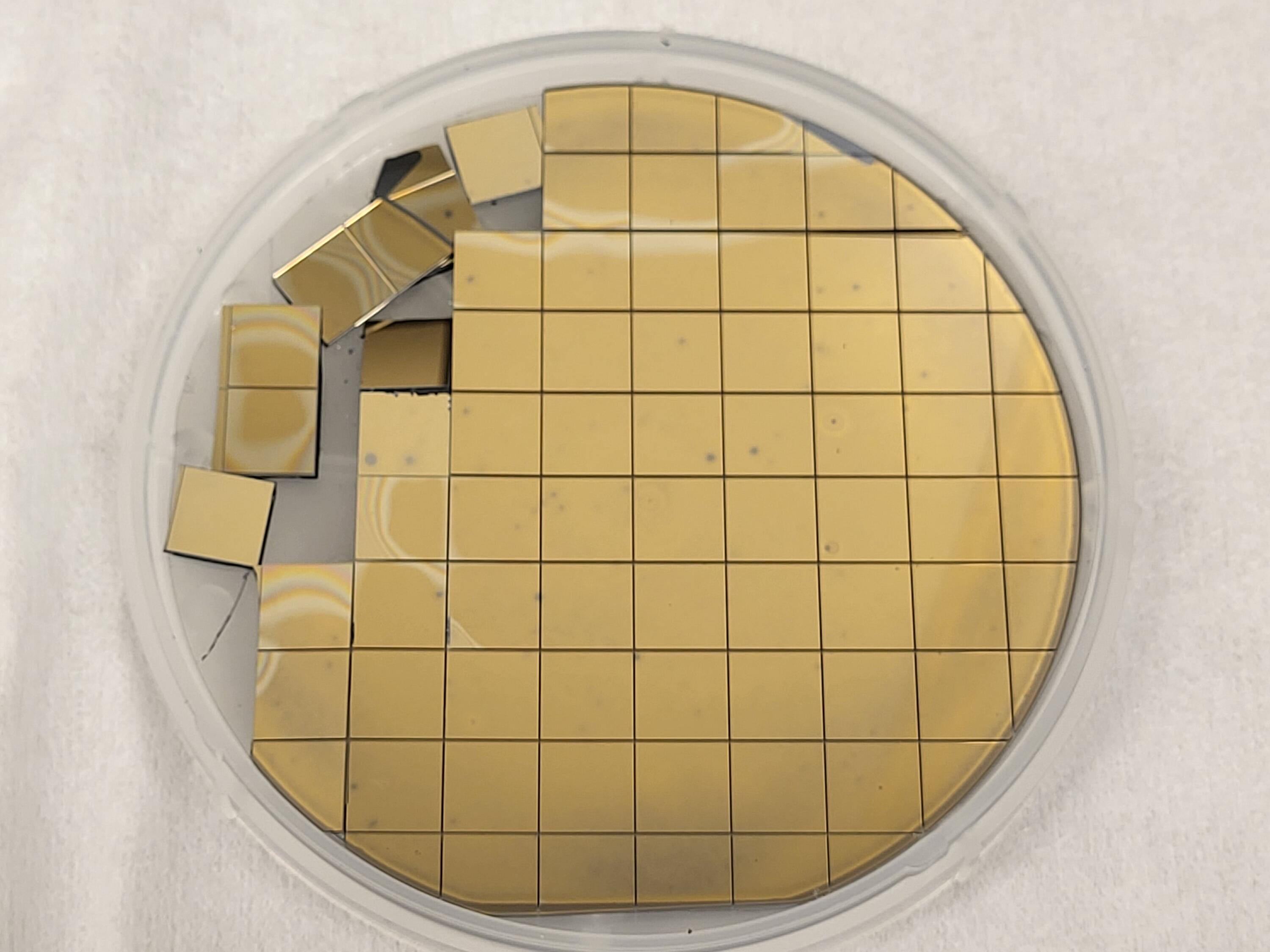
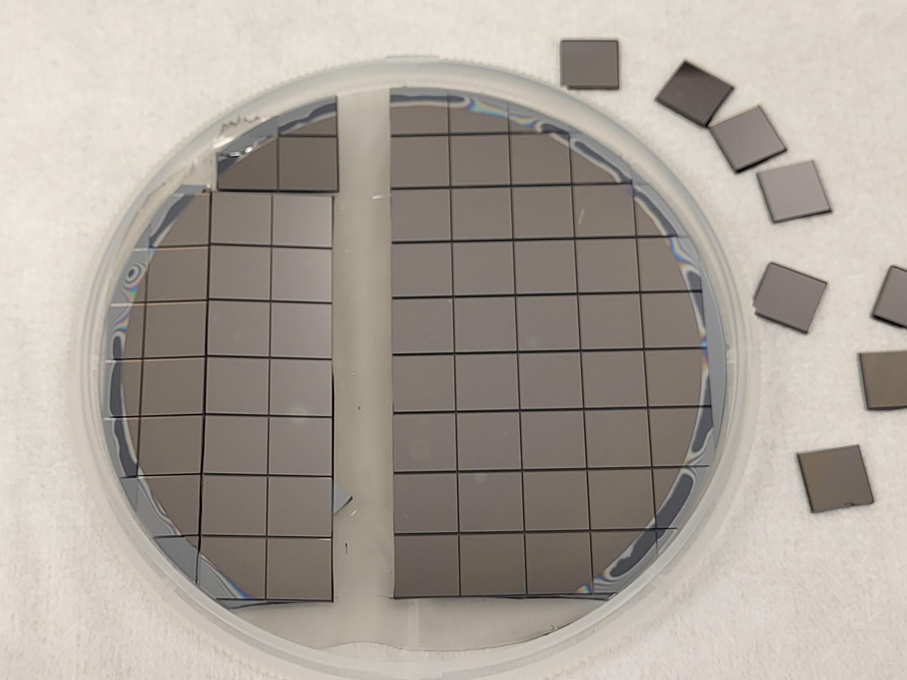
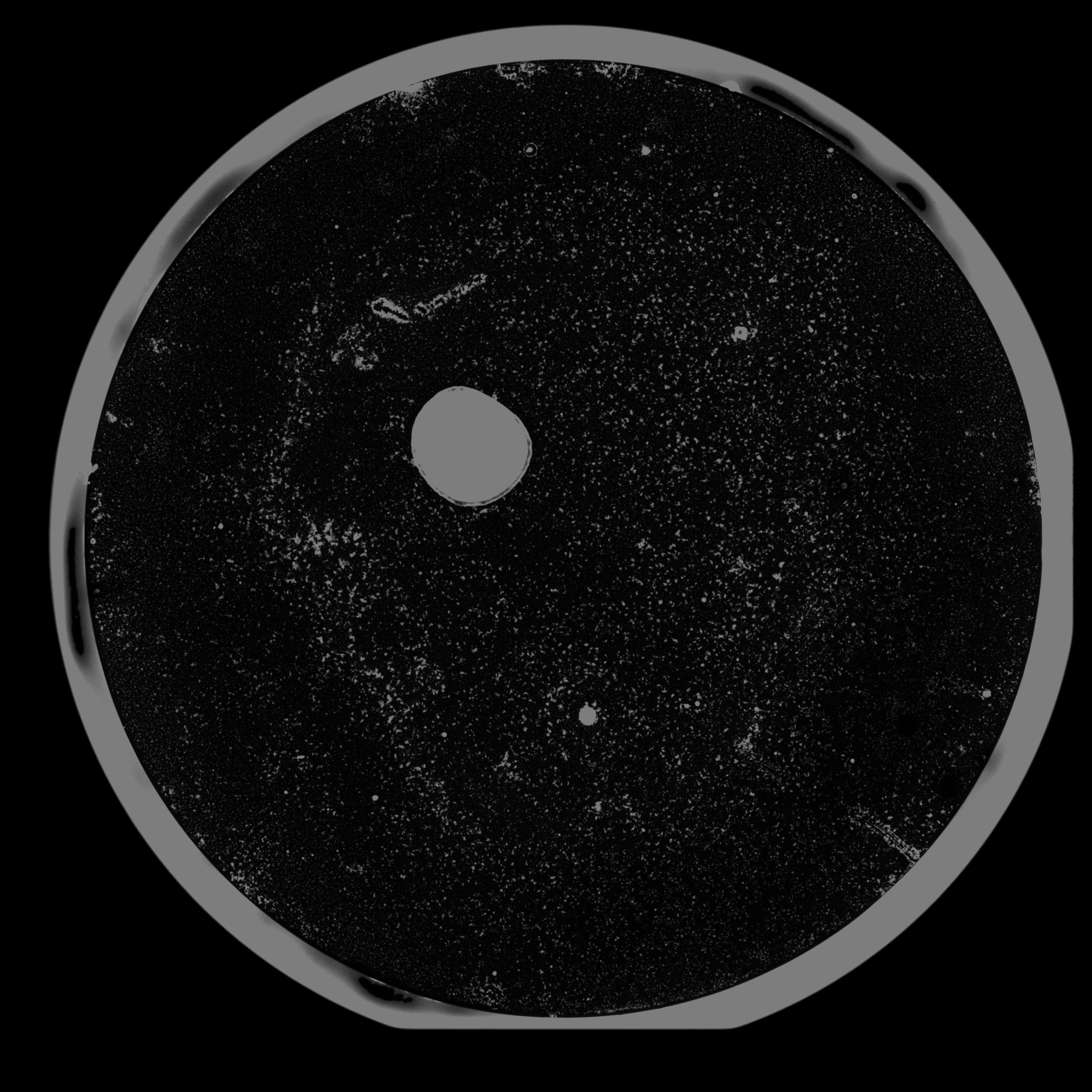
The different bonding techniques were tested to demonstrate the system capabilities. Pairs of Si wafers bonded with Borofloat® 33 were inspected visually and looked under an optical microscope. After direct, eutectic and thermocompression bondings, pairs of wafers were pre-diced into 1 cm x 1 cm pieces with the Disco dicing saw then cleaved. The razor blade insertion test was performed to evaluate the bonding strength qualitatively. For non-transparent bonded pairs, surface acoustic microscopy was performed with a PVA TePla SAM 501HD2 equipped with a 110 MHz 8mm transducer at 25 µm/pixel resolution at Centre de Collaboration MiQro Innovation (C2MI) in Bromont, QC.
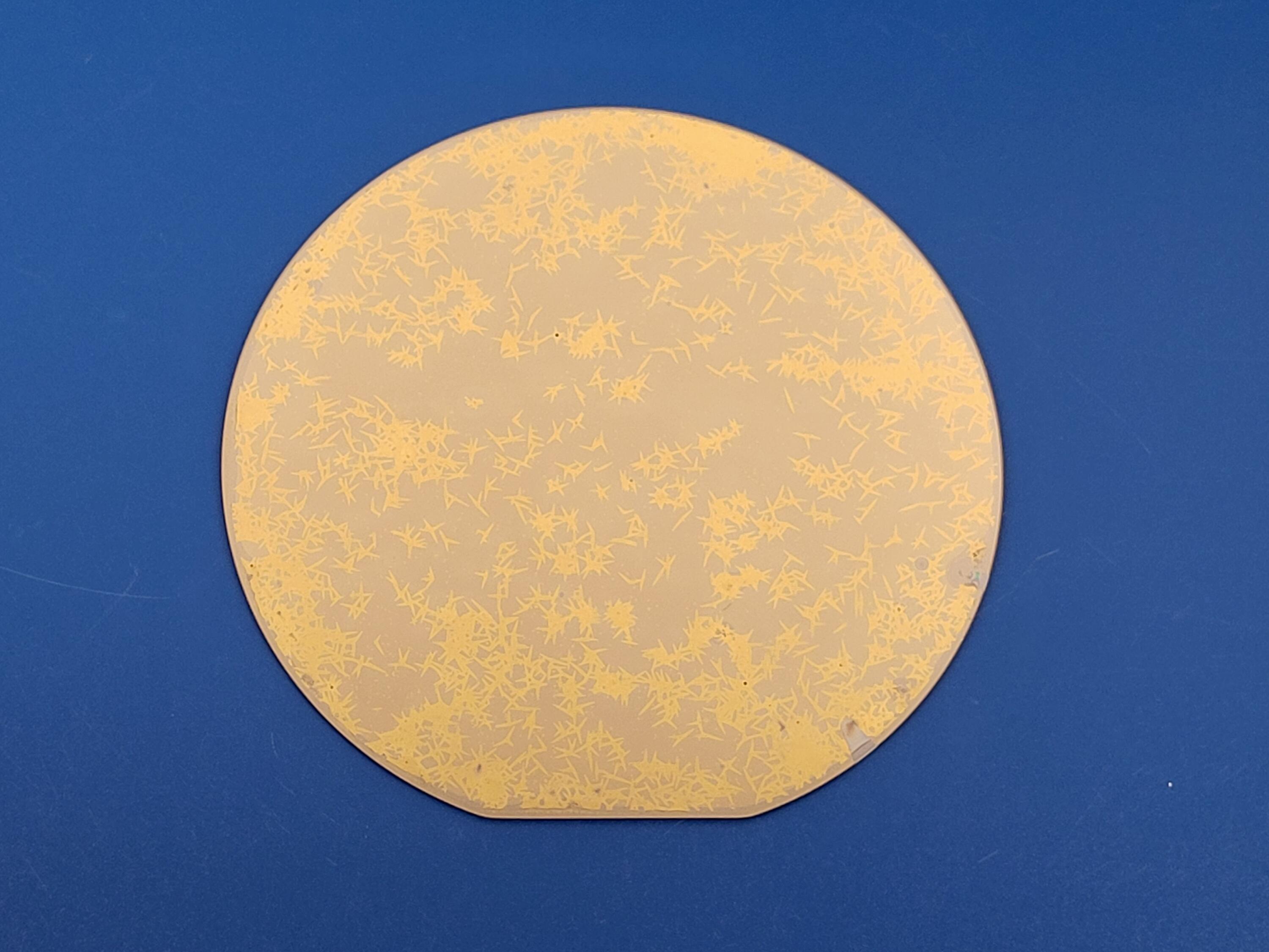
Plasma activated Si-Si direct bonding
Preparation: bare prime 100 mm Si wafers were cleaned in RCA1 solution for 15 min, rinsed and dried in a spin-rinse dryer (SRD), exposed to O2 plasma in the YES downstream plasma cleaner using 500 RF power at 25°C with a 50 sccm O2 flow rate and a pressure maintained at 800 mTorr for 10 min for surface activation, and finally rinsed and dried again in the SRD to remove any potential particle.
Bonding parameters: pairs of Si wafers two wafers were manually pre-bonded at room temperature in clean room air ambient right after the second rinse then were bonded with a force of 7 kN at 370°C under vacuum for 2 hours in the SB6 wafer bonder.
Results
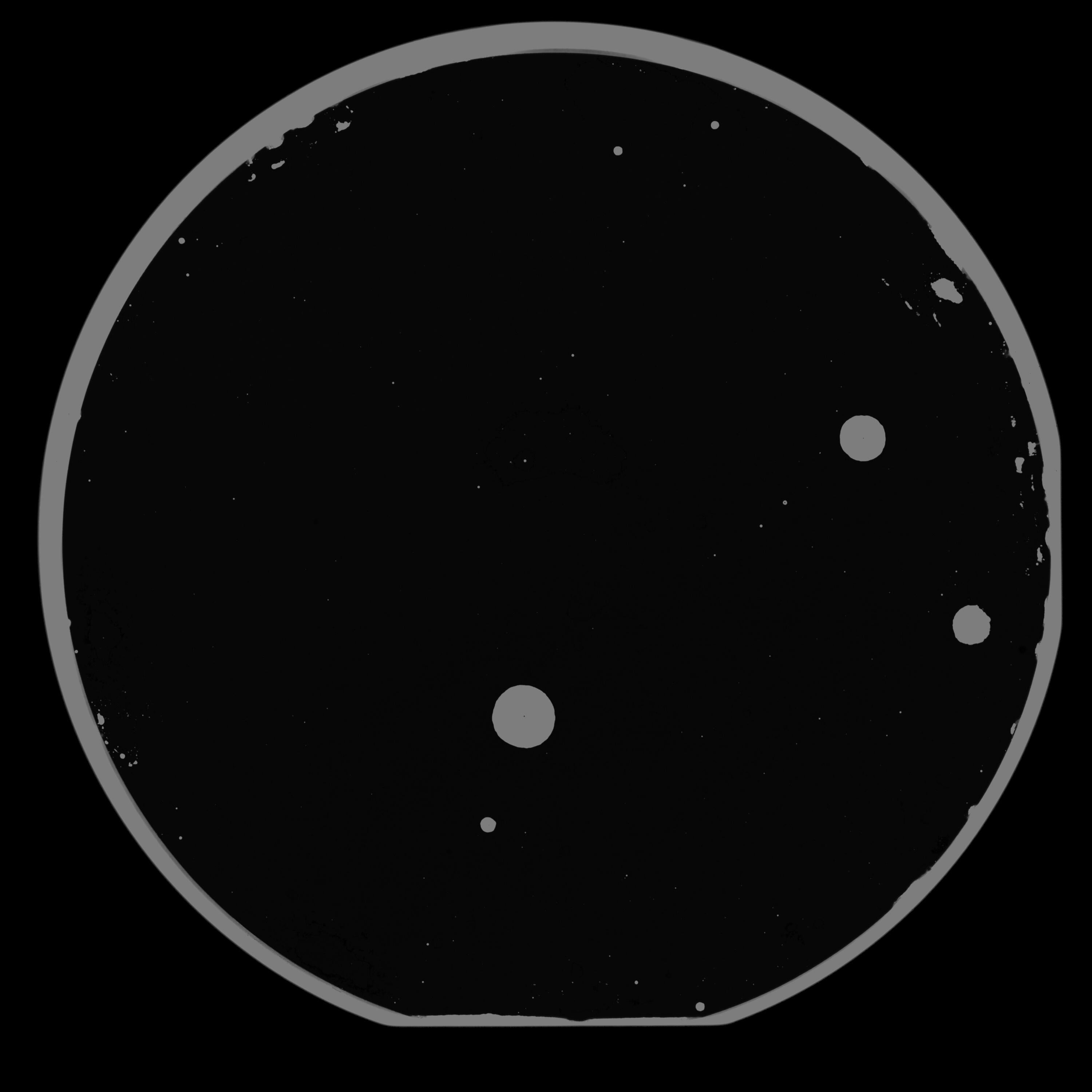
Excluding the edges where the bonding is weak, all the pieces did not separate during the cut and could barely debonded with the blade without breaking. The acoustic image of a second bonded pair shows four macroscopic voids. The largest one is few cm with a particle and a scratch probably due to mishandling. Excluding the largest void, the center is bonded properly but a large number of microscopic voids below 1 mm are present around. These voids and are probably due to desorption of water and hydrogen during annealing in the bonding process and affect the bonding energy. Void-free interface is possible by optimizing the plasma activation [1-2]. The use of the spacers to keep the wafers seperated until the wafer bonder is under vacuum could help desorb water [3].

Acoustic image of plasma activated Si-Si interface

Glass-glass direct bonding
Preparation: bare 100 mm Borofloat wafers were cleaned in piranha solution 4:1 for 15 min, rinsed and dried in a spin-rinse dryer.
Bonding parameters: Two wafers were manually pre-bonded at room temperature in clean room air ambient then bonded with a force of 3 kN at 550°C for 30 min under vacuum.
Results
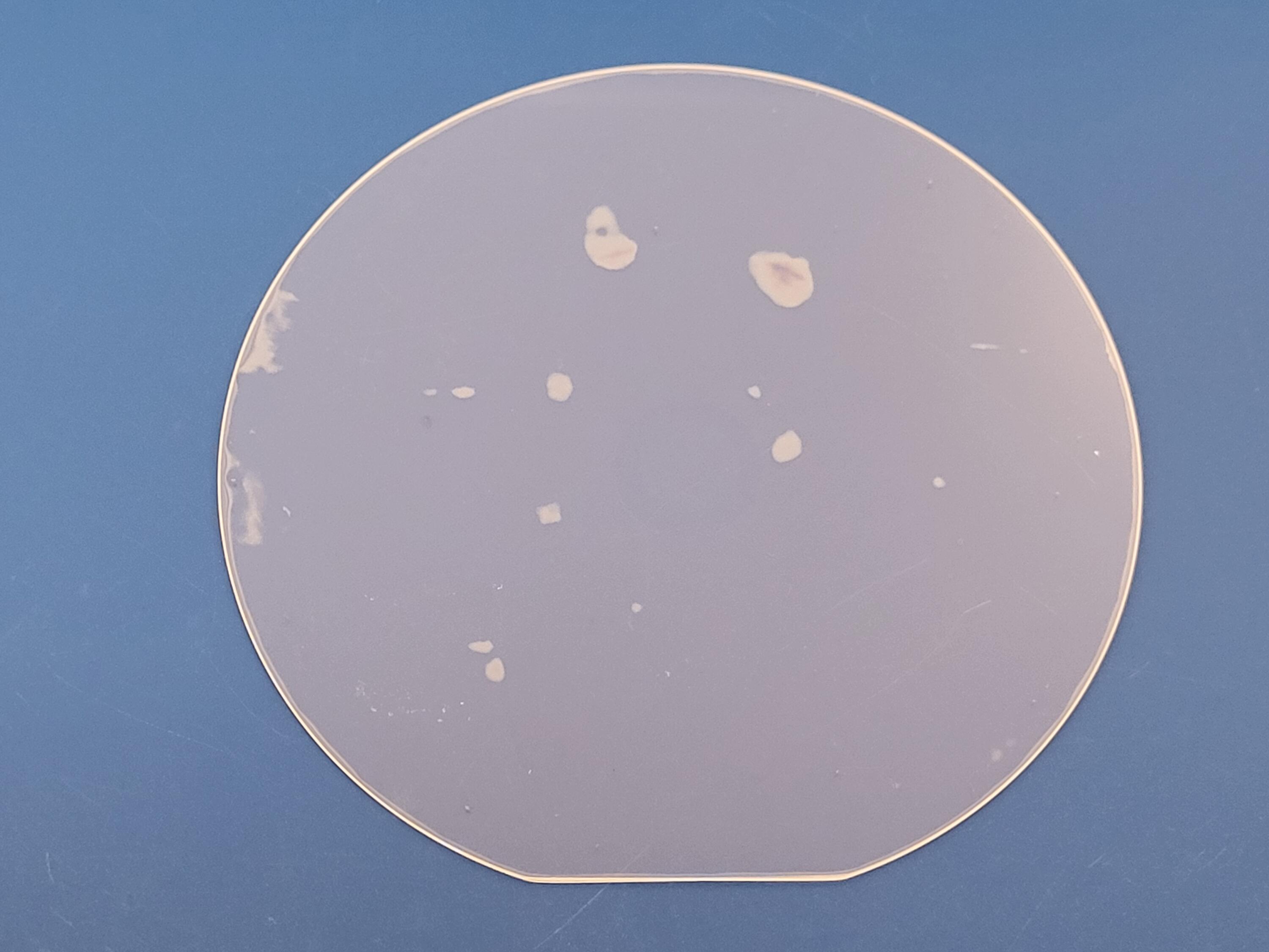
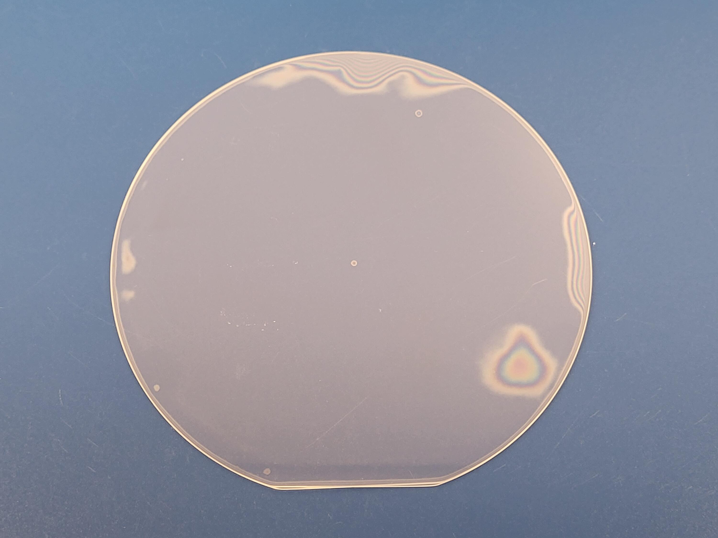
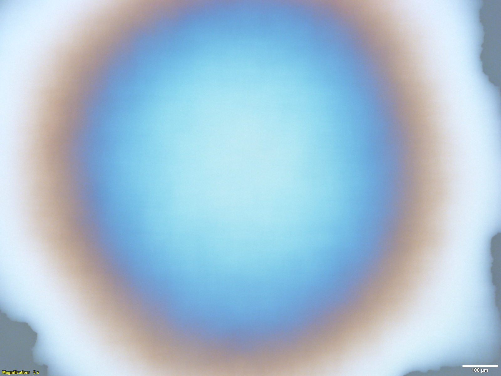
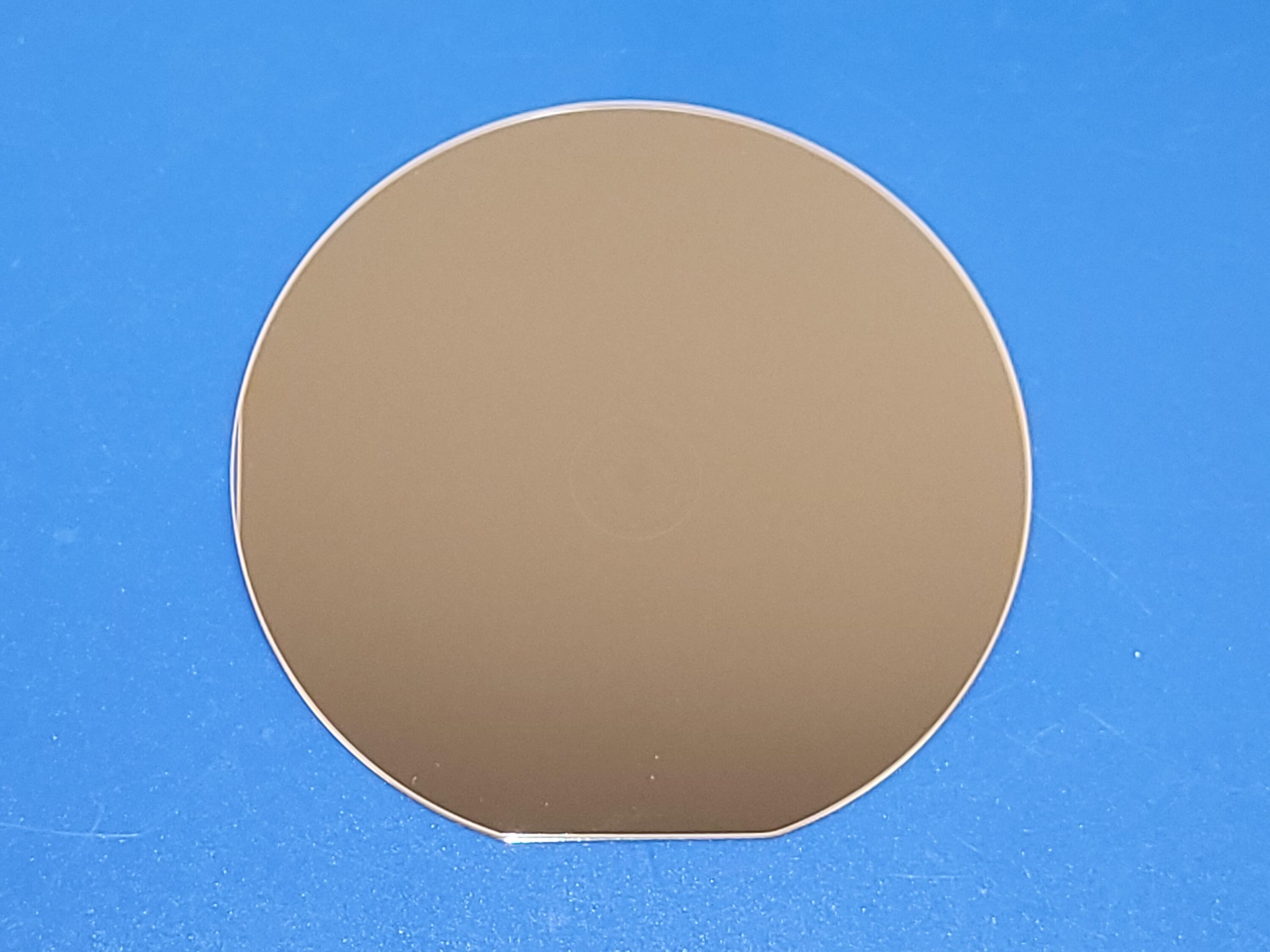
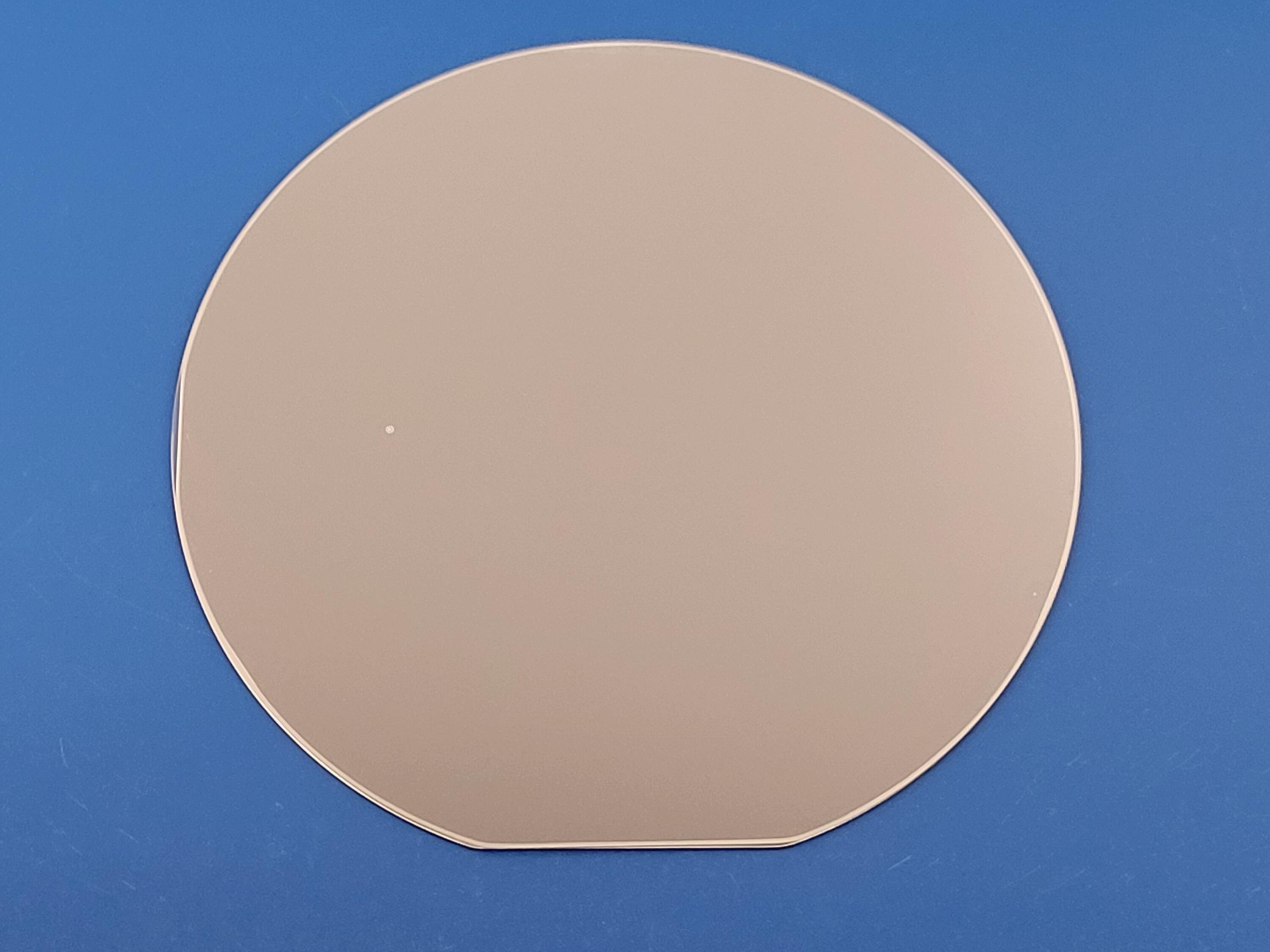
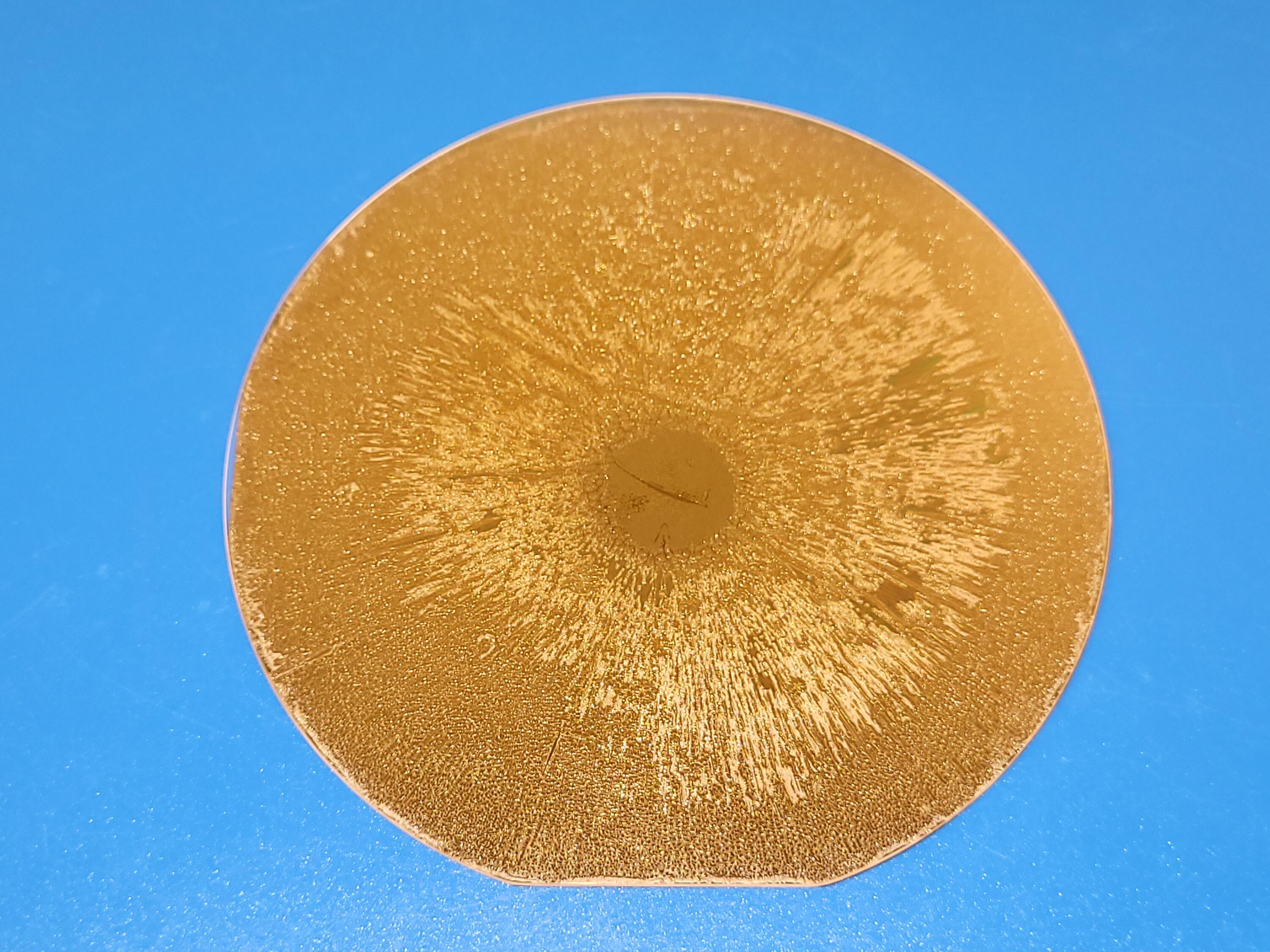
The bonded pair shows few voids by transparency. No particles could be seen in these voids under the microscope, they could originate from air trapped during pre-bonding. A mark of the size of the center pin was left on the surface of the Borofloat wafer and some whitish haze was seen due to sodium contamination of the SiC tool plate during anodic bonding. The use of a plate made of graphite between the between the stacked wafers and the SiC bond plate will prevent these issues.

Bonded pair of Borofloat wafers with SiC tool plate

Bonded pair of Borofloat wafers with intermediate graphite plate

Optical image of a void at the glass-glass interface
Gold-silicon eutectic bonding
Preparation: Borofloat wafers were cleaned in piranha 4:1 for 15 min then rinsed and dried in an SRD. 20 nm Ti/100 nm Au or 20 nm Ti/40nm Pd/100 nm Au were deposited in the Angstrom e-beam evaporator or 20 nm Ti/40 nm TiN/100 nm Au was deposited the AJA sputtering system. For acoustic imaging, 20 nm Ti/40 nm TiN/100 nm Au were sputtered on a silicon wafer with 60 nm thermal oxide. Prior bonding, native oxide was removed from a prime Si wafer in BOE 10:1 for 45 s then rinsed and dried in a spin-rinse dryer.
Bonding parameters: the wafers were bonded with a force of 3 kN at 400°C under vacuum for 20 min. The heating/cooling was controlled over 350°C with a ramp of 5°C/min.
Results
The bonded pairs with Ti/Au and Ti/Pd/Au layers have a weak bond strength as several pieces got separated during dicing. Interference fringes due to weak bonding energy could be seen and the pieces could be easily debonded with the blade inserted. The Ti adhesion layer clearly changed color after bonding with no diffusion barrier and with Pd layer, which indicates that the Pd did not prevent Au-Ti interdiffusion and the metallic layers peeled off from the glass substrate [4]. The formation of dentrites is also observed. This formation likely occured during the cooling process and prevents the formation of the Au-Si alloy needed for strong bonding [5] .
The pairs with TiN diffusion barrier show a slight change in colour of the Ti layer in few spots but all the diced pieces stayed bonded. The acoustic image of the bonded Si wafers shows micro voids probably due to the density mismatch between Si and liquid eutectic Au-Si alloy. The use of an amorphous Si layer on the Si wafer can prevent the formation of voids and craters at the Au-Si interface [6].

Eutectic Au/Si bonded pair of Borofloat/Si wafers with no diffusion barrier

Optical image of the Au/Si eutectic bonded interface with no diffusion barrier

Au/Si eutectic bonded pair of Boroflat/Si wafers bonded with Pd diffusion barrier after dicing and cleaving

Au/Si eutectic bonded pair of Boroflat/Si wafers bonded with TiN diffusion barrier after dicing and cleaving

Acoustic image of eutectic Au-Si interface with TiN diffusion barrier

Gold-gold thermocompression bonding
Preparation: prime Si wafers with 60 nm thermal oxide were cleaned in piranha 4:1 for 10 min then rinsed and dried in an a spin-rinse dryer. 20 nm Ti/100 nm Au were deposited on the Si wafers in the Angstrom e-beam evaporator.
Bonding parameters: the wafers were bonded with a force of 10 kN at 270°C under vacuum for 20 min.
Results
With the edge of the wafers excluded, all the diced pieces show good bond strength and could not be unbonded with the blade insertion test. The acoustic image shows a bonding interface of relatively good quality with few macroscopic voids. The large voids are clearly due to a particle seen at their center. Defects due to handling with wafer tweezers can be seen.

Acoustic image of Au-Au thermocompression interface
Anodic bonding
Preparation: a prime Si wafer and a Borofloat wafer were cleaned in piranha 4:1 for 10 min then rinsed and dried in a spin-rinse dryer. 20 nm Ti/100 nm Au were deposited on the Si wafers in the Angstrom e-beam evaporator.
Bonding parameters: the wafers were bonded with a force of 1 kN at 310°C and 1000 V under vacuum until the anodic current drops below 1.5 A.
Results
Visual inspection shows a good bonding interface with few defects. A white ring of the size of the center pin is left and is likely made of sodium that depletes the Borofloat glass. This residual contamination can be problematic where optical transparency is important like for microfluidic applications. The use of a graphite electrode prevents this issue.

Anodic bonded pair of Boroflat/Si wafers with SiC bond plate

Anodic bonded pair of Boroflat/Si wafers with intermediate graphite electrode
Adhesive bonding
Preparation: AZ P4620 or Cyclotene 3022-46 (B-staged bisbenzocyclobutene) was spun on a bare Si wafer then prebaked at 110°C for 80 s and 100°C for 10 min respectively in the Brewer UV spin/bake station. The expected thickness of AZ P4620 and BCB resist is 6 µm and 3.5 µm respectively. A Borofloat wafer was cleaned in piranha 4:1 for 15 min.
Bonding parameters: the coated Si wafers and glass wafers were bonded with a force of 1350 N at 100°C for 30 min and a force of 900 N at 250°C for 2 h respectively.
Results
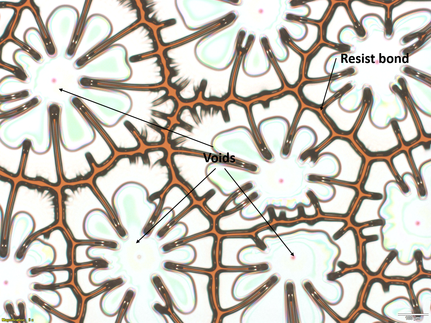
The bonding with AZ P4620 was clearly non uniform when inspected visually. The optical microscope shows microvoids and relatively small bonded areas. The formation of microvoids is likely due to release of nitrogen from diazonaphthoquinone (DNQ) photoactive compound [7]. Adhesive bonding with BCB is of good quality with two voids created by the presence of particles at the edge. Concentric optical fringes are observable and are probably due to variation of the BCB thickness.

Bonded pair of Borofloat/Si wafers with AZ P4620 photoresist

Optical image of the bond interface with AZ P4620 photoresist

Bonded pair of Borofloat/Si wafers with BCB resist
-
X. X. Zhang and J.-P. Raskin, Low-temperature wafer bonding: a study of void formation and influence on bonding strength, Journal of Microelectromechanical Systems, vol. 14, n° 2, pp. 368-382, 2005. DOI: 10.1109/JMEMS.2004.839027
-
M. M. R. Howlader, F. Zhang and M. G. Kibria, Void nucleation at a sequentially plasma-activated silicon/silicon bonded interface, Journal of Micromechanics and Microengineering, vol. 20, n° 6, 2010. DOI: 10.1088/0960-1317/20/6/065012
-
A. Castex, M. Broekaart, F. Rieutord, K. Landry and C. Lagahe-Blanchard, Mechanism of Edge Bonding Void Formation in Hydrophilic Direct Wafer Bonding, ECS Solid State Letters, vol. 2, n° 6, 2013. DOI: 10.1149/2.006306ssl
-
S. Lani, A. Bosseboeuf, B. Belier, C. Clerc, C. Gousset and J. Aubert, Gold metallizations for eutectic bonding of silicon wafers, Microsystem Technologies volume, vol. 12, pp. 1021-1025, 2006. DOI: 10.1007/s00542-006-0228-6
-
D. Li, Z. Shang, Y. She and Z. Wen, Investigation of Au/Si Eutectic Wafer Bonding for MEMS Accelerometers, Micromachines, vol. 8, n° 5, p. 158, 2017. DOI: 10.3390/mi8050158
-
P. H. Chen, C. L. Lin and C. Y. Liu, Amorphous Si/Au wafer bonding, Applied Physics Letters, vol. 90, n° 13, p. 132120, 2007. DOI: 10.1063/1.2719025
-
F. Niklaus, P. Enoksson, E. Kälvesten and G. Stemme, Low-temperature full wafer adhesive bonding, Journal of Micromechanics and Microengineering, vol. 11, n° 2, 2001. DOI: 10.1088/0960-1317/11/2/303
Acknowledgements
This new capability was funded by Canada Foundation for Innovation (CFI) John R Evans Leaders Fund project number 38914 "Taking superconducting electronics to the next level of integration". Matching funds were provided by the Ontario Research Fund. This project was lead by Chris Wilson, Matteo Mariantoni and Raafat Mansour. Additional funding was provided by David Cory.