Background
Organic electronics can be manufactured at lower cost compared to conventional silicon-based electronics and are suitable for widespread applications such as: displays, radio-frequency identification (RFID) tags, chemo/biosensors, memory devices, solar cells, photodiodes, thermoelectric devices, and batteries. In addition, organic semiconductors can be processed at low temperatures and deposited on plastic substrates to enable lightweight, flexible, and ultra-thin electronic devices. However solution-processed organic semiconductors, have shown insufficient electronic performance as compared with inorganic semiconductors. For example, the charge carrier mobility of solution-processed organic semiconductors is typically lower than 1 cm2V-1s-1, which is inadequate as channel semiconductor materials in organic thin film transistors (OTFTs) for many target applications. Therefore there is a need to develop solution-processable organic semiconductors, including monomers, oligomers and polymers, with mobility greater than 0.5 cm2V-1s-1.
Description of the invention
Waterloo researchers have developed monomelic, oligomeric, or polymeric semiconducting organic compounds comprising a fused-ring moiety, which can be used as high performance organic semiconductors for (OTFTs), organic photovoltaics (OPVs), sensors, and other electronic devices. The semiconductor materials may also be a mixture or blend comprising one or more of the above organic semiconducting compound and one or more compounds or polymers. These material have semiconducting, charge transport, hole transport, electron transport, hole blocking, electron blocking, electrically conducting, photoconducting or light emitting properties, which can be used for displays, RFID tags, smart labels, sensors, and solar cells.
Advantages
Our organic semiconducting material shows mobility of greater than 0.5 cm2V-1s-1, and it can be processed at low temperatures and deposited on plastic substrates to enable lightweight, flexible, and ultra-thin electronic devices. It has low cost production using the solubility properties of the compounds and the processibility of large surfaces.
Potential applications
Our semiconductor materials could be used in: organic field effect transistors (OFET), thin film transistors (TFT), integrated circuits (IC), logic circuits, capacitors, radio frequency identification (RFID) tags, devices or components, organic light emitting diodes (OLED), organic light emitting transistors (OLET), flat panel displays, backlights of displays, organic photovoltaic devices (OPV), organic solar cells (OSC), photodiodes, laser diodes, photoconductors, organic photodetectors (OPD), electrophotographic devices, organic memory devices, sensor, charge injection layers, charge transport layers, polymer light emitting diodes (PLEDs), Schottky diodes, antistatic films, and polymer electrolyte membranes.
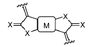
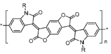
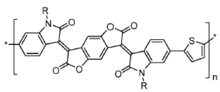
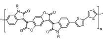
Exemplary semiconductors containing a monomer, oligomer or polymer comprising fused-rings moiety repeat units
Reference
8810-7394
Inventor(s)
Yuning Li
Patent status
U.S. Patent application # 61/724,461 WO 2014/071524, PCT/CA2013/050854
Stage of development
Proven prototype & ongoing development