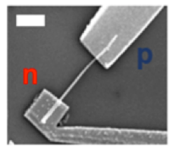
Researchers have found a new method to grow high-quality, defect-free material for nanowire p-n junctions, resulting in better electrical contacts for quantum light-emitting diode (LED) devices.

Nanowires are nanostructures that are grown from gases. Doping agents are used in the growth process to alter the electrical properties of the resulting wire. Previously, nanowire p-n junctions were grown with trimethyl indium and phosphine gases to form indium phosphide (InP), with diethyl-zinc (DEZn) and hydrogen sulfide (H2S) used as p- and n-doping agents during growth. The tips of these InP nanowires are very narrow – approximately 50 nanometers in diameter (a human hair is about 50,000 nm thick). This makes it extremely difficult to make good electrical contacts with InP nanowire tips for the quantum LED.
In this experiment, the researchers gradually changed the material at the nanowire tip from InP to indium arsenide (InAs). InAs nanowires are known for their ability to make good electrical contacts. This gradual change in the nanowire interface allowed for an improved electrical contact of the p-doped side of the nanowire by two orders of magnitude, resulting in enhanced quantum efficiency. This is also the first time that the effect of the introduction of dopants during this new nanowire growth direction on the wire structure has been investigated. This growth direction, 〈100〉, is compatible with current semiconductor technologies.
“Solving this decade-old electrical contact issue is a step towards developing quantum devices. One example is an electrically driven nanodevice that converts single electrons generated by a quantum dot to photons,” said contributing IQC faculty member Michael Reimer, also a professor in the Department of Electrical and Computer Engineering. “From here we can scale up to a device that transfers entanglement. Ultimately, the goal is to build a quantum device that interfaces stationary and flying qubits.”
This research also has implications for quantum detectors, solar cells and other energy conversion applications. The improved electrical contact on the p-side leads to lower resistance of energy flow and a more efficient extraction of the electric current required to generate power.
Reimer collaborated with an international team of researchers from Eindhoven University of Technology, Delft University of Technology, Philips Innovation Services Eindhoven, Université de Toulousse and the Royal Institute of Technology. Their results High-Yield Growth and Characterization of 〈100〉InP p-n Diode Nanowires appeared in Nano Letters on April 5.