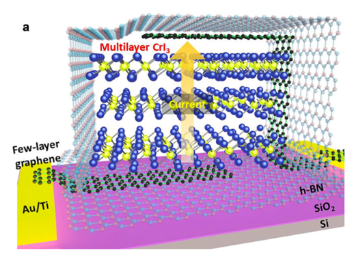
Schematic of the magnetic tunnel junction created by the researchers. The hexagonal boron nitride (h-BN) enclosure protected the chromium tri-iodide from environmental effects.
A team of IQC researchers led by faculty member Adam Wei Tsen and postdoctoral fellow Hyun Ho Kim, in collaboration with the Renmin University of China, demonstrated an electronic device with an extremely large response to a magnetic field by using a combination of two-dimensional quantum materials. The size of this effect was unexpected, and may provide avenues for further development of quantum technologies.
Quantum materials have exotic properties that can help build novel devices. Two-dimensional (2D) materials are a case in point: they are only a few atoms thick and often exhibit different properties than their 3D counterparts.
“Imagine stripping individual compounds down to the single layer limit, and then artificially recombining them to form heterostructures,” said Tsen. “These are new material systems that cannot be directly grown. When you put together different materials like this, new physical phenomena can emerge.”
The researchers observed a one million percent tunnel magnetoresistance in a device called a magnetic tunnel junction made with chromium tri-iodide (CrI3), graphene, and boron nitride. “At first, we just wanted to understand the magnetic properties of CrI3, which is what this device geometry would let us do,” said Tsen, also a professor in the Department of Chemistry in the Faculty of Science. “When we applied a small magnetic field, we saw a huge change in device resistance, and so we decided that this was something worth investigating.”
Magnetic tunnel junctions typically consist of two ferromagnets (inherently, strongly magnetic metals) separated by a thin layer of insulator. When a voltage is applied across the junction, electrons can actually tunnel through the ultra-thin insulator, thanks to quantum mechanics. Switching between parallel and antiparallel magnetizations in the ferromagnets changes electrical resistance in the insulator from low to high. This is tunneling magnetoresistance.
Magnetic tunnel junctions are used in magnetoresistance random access memory (MRAM). By assigning a 0 and a 1 to the high and low resistance states, MRAM can be used as both computer storage and memory.
Interested in what would happen if the semiconductor itself was layered and magnetic, the researchers made the magnetic tunnel junction by manually placing 2D layers of the magnetic semiconductor CrI3 between graphene electrodes. When a voltage was applied across the tunnel junction, electrons quantum-tunneled through the thin layer of CrI3.
In a low-temperature environment, the team then introduced a magnetic field. That is when something interesting happened: the electric current passing through the junction increased by one million percent.
Coupling between layers of 2D CrI3 is, unlike with its 3D counterpart, antiferromagnetic: each layer has an opposite spin to the one above and below it. This creates a high barrier to electron tunneling. When the researchers introduced a magnetic field, it aligned the spins of each layer, which reduced the tunnel barrier and allowed for a dramatically reduced electrical resistance of the semiconductor.
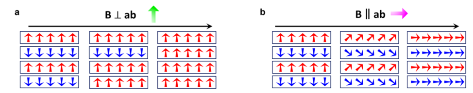
Progression of the polarization of spins in each layer of chromium tri-iodide with the introduction of a magnetic field. Diagram a) represents the change with a perpendicular magnetic field, while b) represents the change with a parallel one.
The researchers observed magnetoresistance several orders of magnitude larger than that of current tunnel junctions used in commercially available MRAM. The observation of this sizable magnetoresistance and fine spin control opens up a path for further research with this quantum material that could lead to advances in spintronics.
The paper, One Million Percent Tunnel Magnetoresistance in a Magnetic van der Waals Heterostructure, appeared in Nano Letters.
This research was undertaken thanks in part to funding from the Canada First Research Excellence Fund.