The G2N facility has recently installed new processing and characterization tools as part of its expansion from a $5.7M CFI-ORF Innovation Fund Project. The funding supports the new Facility for Functionally Advanced Sensor Technology (FAST) within G2N to support the efforts of the lab in the development of organic and inorganic semiconductor devices.
The recent additions include:

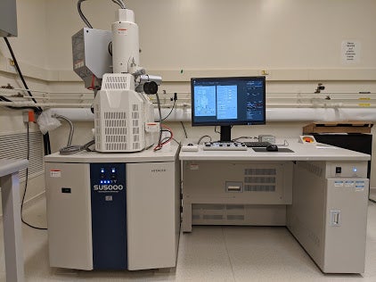
1. A Hitachi SU5000 field-emission scanning electron microscope with a Lifeforce LF-2000 nanomanipulation system. The new SEM and nanomanipulator will support on-going work in thin-film flexible electronics and expand the labs capabilities to characterize two-dimensional transition-metal dichalcogenide (TMD) materials.

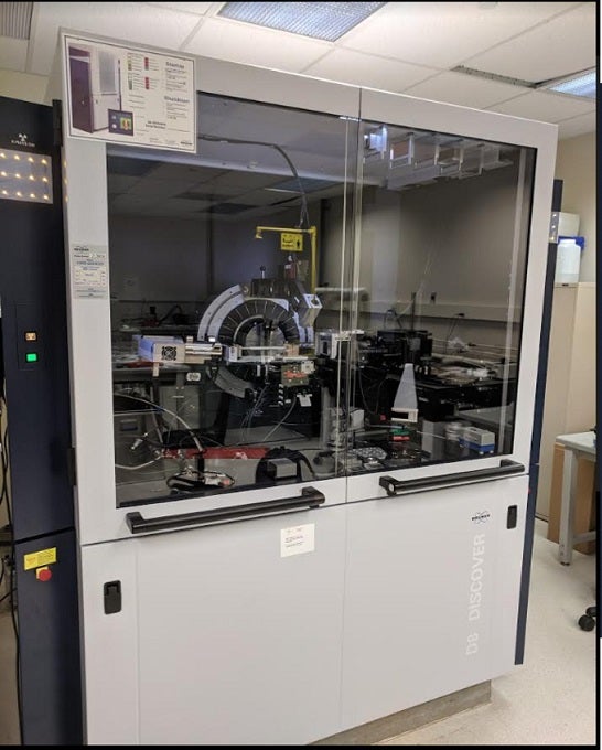
2. A Bruker D8 Discover x-ray diffractometer capable of two-dimensional spatial mapping, grazing incidence diffraction for in-plane characterization and phase analysis of crystal domains in thin-film materials. This tool will support and expand the research efforts in polymeric materials and two-dimensional TMD semiconductors.

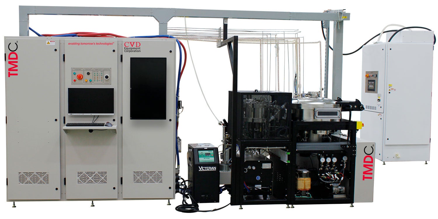
3. A CVD Inc. multi-chamber cluster tool with chemical vapor deposition (CVD) and atomic layer deposition (ALD) chambers. The custom designed reactor allows for the deposition of MoS2 layers by CVD along with Al2O3 and HfO2 dielectric materials by ALD. This tool expands the research capabilities of G2N in the synthesis of two-dimensional materials for next-generation electronic devices.

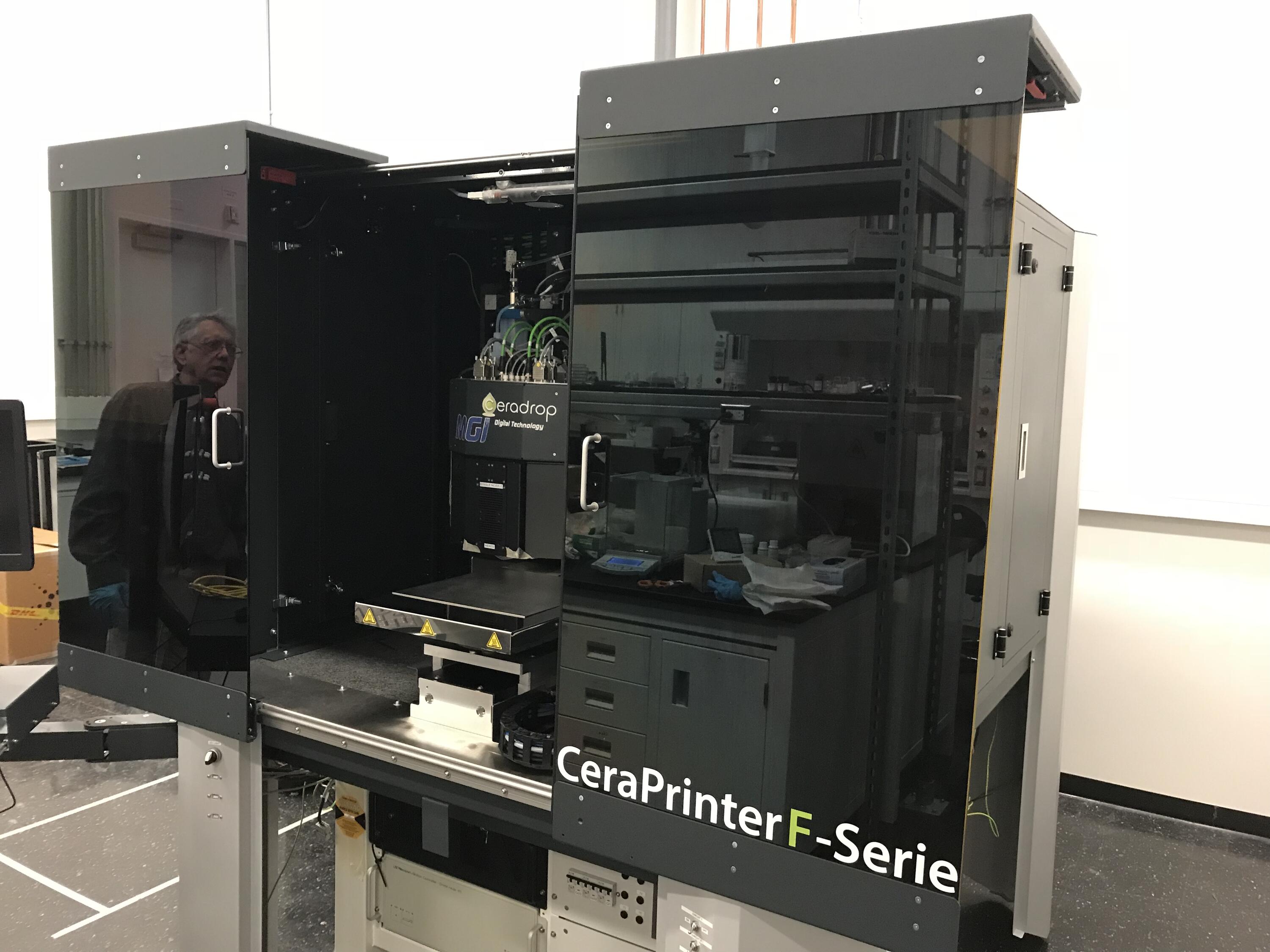
4. A Ceradrop F-Serie Digital Materials Deposition platform for the development of printed flexible electronics. The new printing system is equipped with ink-jet and aerosol-jet printing capabilities to process a wide variety of different electronic inks. The system expands the existing printed electronics research in G2N for the development of flexible electronics applications.
The installation of the new infrastructure will continue through the coming months and announcements will be made as new tools come online.