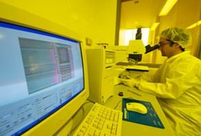
Characterization equipment
The Giga-to-Nanoelectronics (G2N) Centre has a wide variety of thin film device and circuit characterization tools.
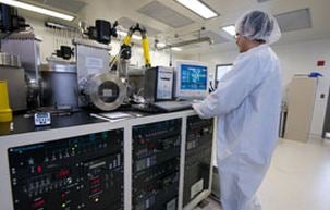
Deposition equipment
The G2N Centre has the deposition capabilities for a variety of semiconductor, dielectric and conductive thin films: amorphous, nanocrystalline and poly-Si, SiOx, SiNx, SiOxNy, SiC, SiCN, ITO, ZnO, Al, Cr, Mo, W, Ta, organic materials (both small molecule and polymers). The maximum substrate size varies form 3 to 12 inches depending on the system.
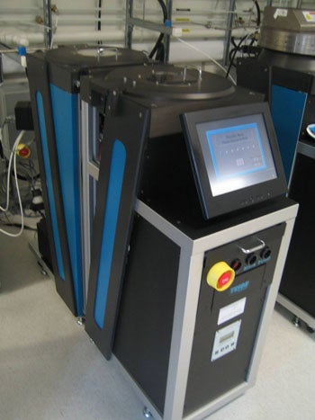
Etching
The G2N Centre has both wet etching and dry etching (F-based, O-based, and Cl-based dry etching (RF,ICP)) capabilities.
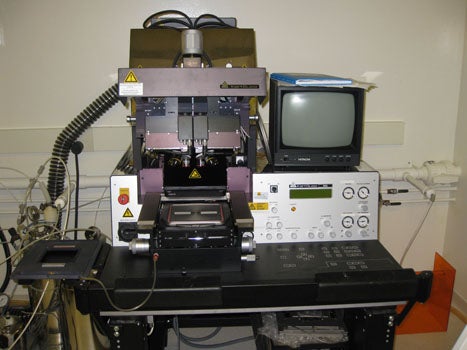
Lithography equipment
The G2N Centre has the ultraviolet (UV) contact lithography capabilities with resolution about 1 micrometer.
Packaging and bonding equipment
The G2N Centre has wafer dicing and wire bonding capabilities.