Faculty members participating in silicon devices and integrated circuits research:
| Hany Aziz | Chris Backhouse (adjunct) | Dayan Ban | Slim Boumaiza |
| Bo Cui | Vincent Gaudet | Karim Karim | Na Young Kim |
| Peter Levine | Omar Ramahi | Chettypalayam Selvakumar | Siva Sivoththaman |
| Lan Wei | William Wong |
The Silicon Devices and Integrated Circuits (SiDIC) area covers several sub-areas including semiconductor materials and processing, modelling and simulation of electronic devices, fabrication technologies for electronic devices, and integrated circuits. The areas of applications are diverse and include high performance IC technologies, large area electronics digital medical imaging applications, flexible electronics, display applications, and photovoltaic energy conversion. SiDIC research benefits from two world-class research facilities, the Giga-to-Nano (G2N) Center and the Centre for Advanced Photovoltaic Devices and Systems (CAPDS). The G2N facility was established in 2000 with a total budget of over $15M, and CAPDS in 2004 with a budget of $12M as a result of two successful CFI innovation Fund projects led by SiDIC professors.
Faculty members in the group consistently hold prestigious research chairs such, NSERC Industrial Research Chairs (DALSA, COMDEV), Canada Research Chairs, NSERC E.W.R. Steacie Fellowship, and the Ontario Research Chair. Faculty members' research within the SiDIC group is strongly supported and funded by major industrial partners (XEROX, KODAK, DALSA, COMDEV, IBM, ATS, and ARISE Tech). There are numerous faculty members actively involved in SiDIC research, and several others from other departments and groups who interact in research in G2N and CAPDS facilities. A list of current research activities include: Bipolar and Field Effect Devices Modeling and experimental process technologies, around SiGe Devices and low temperature and integrable IC technologies, Silicon-on-Insulator technologies and buried silicides, development of cost-effective process technologies for high performance sensors and thin film transistors; design of novel sensors, read-out circuitry, and system architectures; development of transient and steady-state numerical and SPICE models; and integration of the various technology kernels, including assembly and packaging, for high performance optical and X-ray imaging, thin film transistor integration on rigid and flexible substrates, including fabrication of novel device structures, active matrix backplanes for organic light emitting diode (OLED) displays, biomedical x-ray imaging and photon counting, crystalline and thin-film photovoltaic technologies, and next generation nano-Photovoltaic technologies.
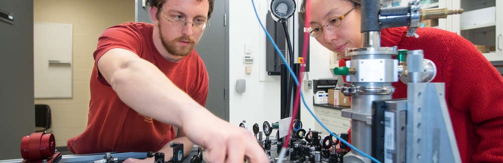
Graduate students acquire hands-on training in many aspects of electronic materials, devices, and integrated circuits and are highly sought-after both by academia and industry after graduation and several have received NSERC doctoral prizes and postdoctoral fellowships.