A new nanoscale diamond structure that better collects and controls light
The novel device produces a ‘nanojet’ of light and holds promise to advance scalable quantum technologies
By Naomi Grosman
Researchers at the Institute for Quantum Computing (IQC) at the University of Waterloo have demonstrated a nanoscale optical device that makes it easier to probe quantum systems with light to enable more efficient quantum sensors and solid-state quantum computing systems. The new device was demonstrated in diamond as a proof of principle.
This optical device has the potential to make quantum sensors better at detecting weak magnetic fields, which could enhance technologies in biomedical imaging or navigation in GPS-denied environments. It could also advance solid-state quantum computing architectures by improving control and readout of individual quantum bits (qubits), and the transfer of quantum information between them.

“Our new approach offers a powerful and practical route to enhance light–matter interaction in solid-state platforms."
-Dr. Behrooz Semnani
Semnani spearheaded the research in Dr. Michal Bajcsy’s group, IQC Faculty and Professor, Department of Electrical and Computer Engineering.
Solid-state quantum platforms such as diamond, silicon carbide, and silicon can host atom-like defects, also known as quantum emitters or color centers, that can serve as qubits. These defects can be initialized, controlled, and read out with laser light, and in many cases can also act as solid-state single-photon sources.
In practice, however, aiming a laser at a single defect can be difficult. Additionally, efficiently collecting the optical signal is challenging because these materials have a high refractive index, causing much of the light emitted by the defects to remain trapped inside the material rather than being collected.
That’s the problem Bajcsy’s group aims to solve with a novel device reported in a new paper Probing Individual Quantum Emitters in Bulk Semiconductors via Photonic Nanojets published in Science Advances.
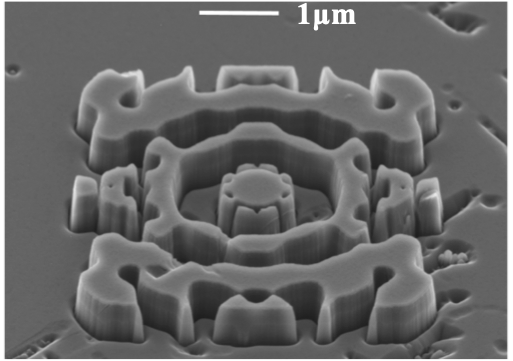
The group used an automated, inverse design approach to optimize the shape of a two-dimensional structure sculpted into a diamond surface. The structure was designed to funnel light into a highly localized nanoscale beam known as a ‘photonic nanojet’ to isolate and aim at single defects in the diamond crystal. The structure was also optimized to act like an antenna for light to help extract photons emitted by the defects.
To demonstrate this, the group fabricated the structure on a synthetic diamond piece to probe a defect called nitrogen vacancy.

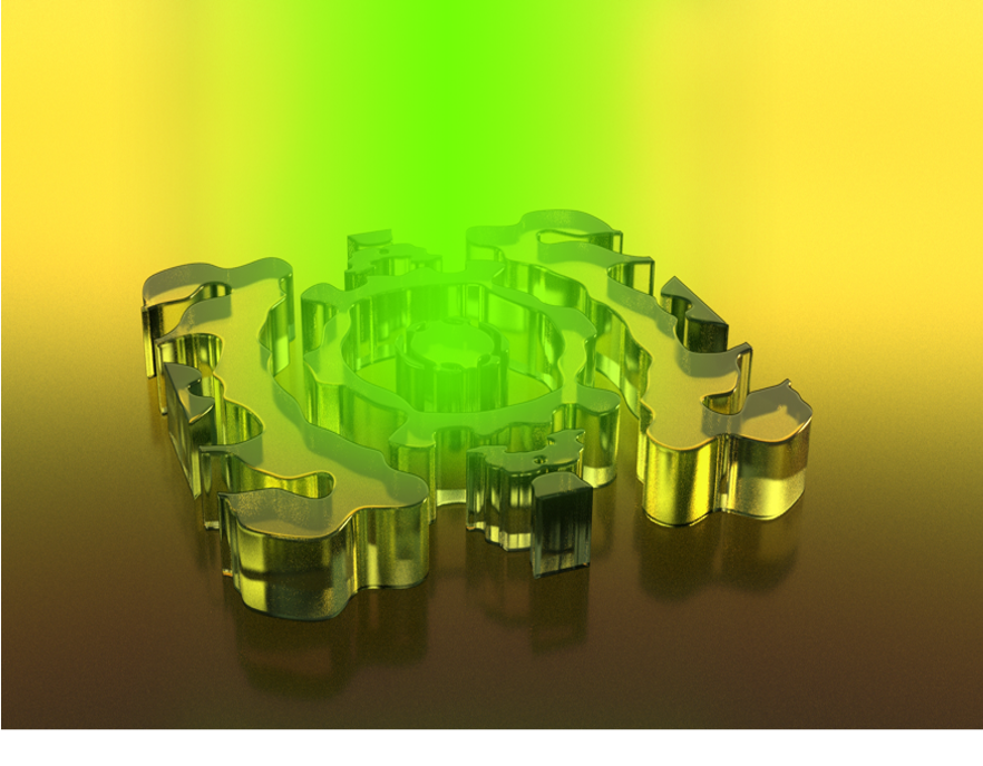
Dr. Michal Bajcsy's group designed a quantum device in diamond that funnels and aims a highly localized beam of photons at single engineered defects in diamond and is optimized to extract photons. Better collecting and controlling light has applications in quantum sensing and solid-state quantum computing architecture.

The group used an automated, inverse design approach to optimize the shape of a two-dimensional structure sculpted into a diamond surface. The device size is about 1 micrometre - 100 times smaller than the width of a human hair.

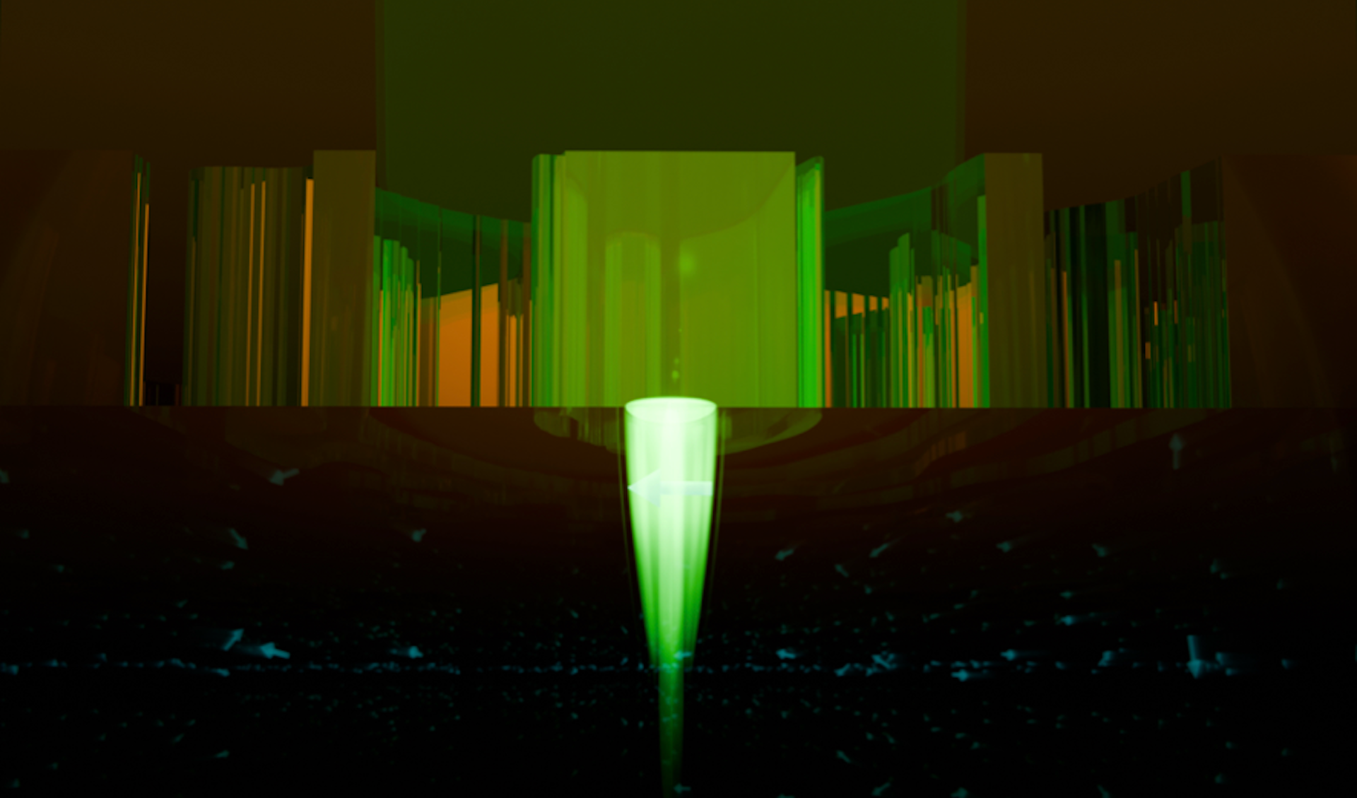
Side view showing the 'Photonic Nanojet' funneling light.
“Our nanojet structure introduces a lot of new benefits but uses a very common fabrication technique without the difficulties associated with some of the previously reported structures used to couple light in and out of quantum emitters in diamond and other materials," says Semnani, who was IQC Research Associate at the time of the research. "This provides a path towards enhanced efficiency.”
Bajcsy says that they are hoping to expand this work into other materials that contain individual defects suitable for sensing or as qubits.
“With most semiconductor materials, it’s hard to extract photons emitted by embedded defects and we hope that our nanojet structures will enable studies and new applications of less common emitters.”
- Dr. Michal Bajcsy, IQC Faculty and Professor, Department of Electrical and Computer Engineering.

He adds that the results allowed addressing individual defects even in low-quality diamond crystals, instead of expensive high-purity diamond samples often used in quantum experiments. This will help with the development of low-cost quantum sensors.
“The device’s simple fabrication process, minimally invasive geometry, and compatibility with reliable device manufacturing make it especially attractive for scalable quantum technologies,” Semnani says.
The device was fabricated at the Quantum-Nano Fabrication and Characterization Facility at the University of Waterloo. The group says access to the facility’s advanced tools, technical support and adaptable processes gave them a flexible and robust fabrication ecosystem to develop new ideas and iterate the device concept.
The paper’s other co-authors are Sai Sreesh Venuturumilli, IQC PhD student; Dr. Mohammad Soltani, IQC post doc; Dr. Pratik Adhikary, IQC post doc; Abdolreza Pasharavesh, IQC PhD student; Nikolay Videnov IQC PhD student; Dr. Paul Anderson, IQC Post doc; Vinodh Raj Rajagopal Muthu, IQC alumni; and Supratik Sarkar, IQC alumni.
The research was supported in part by the Canada First Research Excellence Fund through the Transformative Quantum Technologies (TQT) program at IQC.
Une nouvelle structure nanométrique en diamant, plus efficace pour capter et diriger la lumière
Le nouvel appareil, qui produit un « nanojet » de lumière, s’annonce prometteur pour le développement de technologies quantiques évolutives
À l’Institut d’informatique quantique (IQC) de l’Université de Waterloo, des chercheurs ont présenté un appareil optique nanométrique qui facilite l’examen de systèmes quantiques au moyen de la lumière, en vue d’améliorer les capteurs quantiques et les systèmes d’informatique quantique à l’état solide. Ce nouveau dispositif a fait l’objet d’une démonstration de faisabilité sur du diamant.
L’appareil optique a le potentiel d’aider les capteurs quantiques à mieux détecter les champs magnétiques faibles, et d’ainsi bonifier les technologies d’imagerie biomédicale ou de navigation dans des environnements sans GPS. Il pourrait également contribuer aux architectures d’informatique quantique à l’état solide en raffinant le contrôle et la lecture de bits quantiques individuels (qubits), et au transfert d’information quantique entre eux.
« Notre nouvelle approche ouvre une avenue efficace et pratique pour améliorer les interactions entre la lumière et la matière dans les plateformes à l’état solide. »
-Behrooz Semnani
M. Semnani a dirigé les recherches menées par le groupe de Michal Bajcsy, professeur à l’IQC et au Département de génie électrique et informatique.
Les plateformes à l’état solide, telles que le diamant, le silicium et le carbure de silicium, peuvent présenter des défauts atomiques, aussi appelés émetteurs quantiques ou centres colorés, qui servent de qubits. Ces défauts peuvent être créés, contrôlés et détectés à l’aide d’une lumière laser et, dans de nombreux cas, font aussi office de sources de photons uniques à l’état solide.
Néanmoins, en pratique, il peut s’avérer ardu de pointer un laser sur un seul défaut. Il est également compliqué de capter efficacement le signal optique, car ces matériaux possèdent un indice de réfraction élevé, qui fait en sorte que la lumière émise par les défauts reste piégée à l’intérieur du matériau.
C’est le problème que le groupe du Pr Bajcsy cherche à résoudre, au moyen d’un appareil qu’il a présenté dans un récent article intitulé « Probing Individual Quantum Emitters in Bulk Semiconductors via Photonic Nanojets » (Étude d’émetteurs quantiques individuels dans des semiconducteurs massifs à l’aide de nanojets photoniques) et publié dans Science Advances.
Le groupe a adopté une approche de conception inverse automatisée pour optimiser la forme d’une structure en deux dimensions, sculptée à la surface d’un diamant. Cette structure a été conçue pour canaliser la lumière dans un faisceau nanométrique extrêmement précis – appelé « nanojet photonique » – qui cible et isole les défauts individuels du cristal de diamant. La structure a aussi été améliorée pour agir comme une antenne attirant la lumière et permettant d’extraire les photons émis par les défauts.
Aux fins de la démonstration, le groupe a fabriqué la structure sur un morceau de diamant synthétique pour étudier un défaut appelé azote-lacune.
« Notre nanojet présente nombre de nouveaux avantages, et qui plus est, sa structure repose sur une technique de fabrication très courante, qui ne présente pas les difficultés rencontrées par les structures antérieures servant à coupler la lumière entrant et sortant d’émetteurs quantiques dans le diamant et d’autres matériaux, explique M. Semnani, qui était associé de recherche à l’IQC au moment du projet. Cela ouvre la voie à une plus grande efficacité. »
Le Pr Bajcsy et son groupe espèrent élargir ces travaux à d’autres matériaux qui contiennent des défauts individuels adaptés pour la détection ou pour servir de qubits.
« La plupart du temps, il est difficile d’extraire les photons émis par les défauts de matériaux semiconducteurs. Nous croisons les doigts pour que nos nanojets donnent lieu à des études et à de nouvelles applications du côté des émetteurs moins communs. »
– Michal Bajcsy, professeur à l’IQC et au Département de génie électrique et informatique
Il ajoute qu’il leur a été possible d’étudier des défauts individuels même à l’intérieur de diamants de faible qualité, au lieu des échantillons de cristaux extrêmement purs qui sont souvent utilisés pour les expériences quantiques. Cela contribuera à l’élaboration de détecteurs quantiques à bas prix.
« Le processus d’assemblage simple de l’appareil, sa géométrie peu invasive et sa compatibilité avec des procédés de fabrication fiables en font une avenue particulièrement intéressante pour les technologies quantiques évolutives », souligne M. Semnani.
L’appareil a été assemblé à l’Installation de fabrication et de caractérisation quantiques nanométriques à l’Université de Waterloo. Grâce aux outils avancés, au soutien technique et aux processus adaptables de l’installation, le groupe a bénéficié d’un écosystème de fabrication flexible et robuste pour explorer de nouvelles idées et reproduire le concept de l’appareil.
D’autres auteurs ont également contribué à rédiger l’article susmentionné : Sai Sreesh Venuturumilli, doctorant à l’IQC; Mohammad Soltani, chercheur postdoctoral à l’IQC; Pratik Adhikary, chercheur postdoctoral à l’IQC; Abdolreza Pasharavesh, doctorant à l’IQC; Nikolay Videnov, doctorant à l’IQC; Paul Anderson; chercheur postdoctoral à l’IQC; Vinodh Raj Rajagopal Muthu, diplômé de l’IQC, et Supratik Sarka, diplômé de l’IQC.
Ces travaux ont été partiellement financés par le Fonds d’excellence en recherche Apogée Canada, dans le cadre de l’initiative Transformative Quantum Technologies à l’IQC.