Design team members: Drew Guckenberger
Supervisor: C.R. Selvakumar (E&CE)
Background
Deep space and planetary environments within our solar system provide extremely harsh in situ environments for electronics. For example, on mars the temperature cycles each solstice (~24.6 hours) from –120C to 0C. Further, the radiation environment is also a concern both on the planet and in transit from earth, where the spacecraft is exposed to high energy solar and galactic radiation.
The
following
picture,
"Solar
Intensity
&
Space
Probe
Temperature"
from
Dickman
and
Cytrynowicz
(NASA
LeRC)
illustrates
the
temperature
variation
in
direct
sunlight
and
the
energy
flux
that
a
probe
receives
as
is
it
travels
outward
through
the
solar
system.
These
values
are,
of
course,
higher
than
what
a
probe
would
be
exposed
to
when
it
is
shielded
from
the
sun
by
a
planet,
or
other
body.
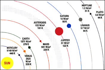
This graphic is very important for two reasons. First of all it shows that the local environmental temperature can become very low even within our solar system in full view of the sun. Secondly it shows that as a probe gets further from the sun the flux of light that can be used to produce solar power decreases (as would be expected for a sphere of expanding radius with a source at its center). This is very important as it points out a problem often referred to as a power spiral. That is, less and less power is available as a probe moves further from the earth, but more and more power is needed in order to keep a probe within the standard temperature ranges (-55C to 125C is the military temperature range). As such, as we move towards exploring the outer planets of our solar system, and even mars, it becomes important to try and minimize the amount of power required for environmental conditioning (in this case heating), as this power can be better used by applying it to actual mission goals. If electronics can operate in the local (in situ) environments, a probe can accomplish more mission goals and be more productive. As well, situations where power is temporarily removed will not pose as significant a threat to the operation of a unit, or system.
There are known techniques for dealing with and predicting radiation effects over normal temperature ranges (-55C to 125C). As well, electronic performance is well understood over this temperature range. What is not well understood is the effect of the temperatures between –55C and –196C (Liquid Nitrogen (LN2) temperature (77K)). There is a gap in the depth of general knowledge in the electronics community in this region. The performance of electronics at these temperatures and an understanding of the phenomena associated with them are crucial for designing and evaluating electronic performance in deep space environments and planetary environments, such as mars. Further, the effect of these low temperatures on radiation susceptibility has never been assessed (that is, the covariance of performance parameters due to simultaneous low temperature and radiation effects). Finally, there are mechanical issues with electronics packaging that must be dealt with so that electronics can survive the large temperature swings experienced in planetary environments when a probe moves from sunlight to shadow (day to night), such as would be experienced each solstice on the martian surface.
Current knowledge indicates that there are problems with minority carrier devices, such as BJTs, that set in somewhere between –55C and -196C (LN2 temperature) due to carrier freeze out. There can also be significant performance degradation for these devices before the carrier freeze-out sets in. The threshold levels where such problems set in are not well known. No such problems are reported for majority carrier devices, such as MOSFETs. In fact, in general, MOSFET performance improves with lower temperature. It is, however, generally accepted in the radiation effects community that, in general, BJTs are less susceptible to radiation effects than MOSFETs. As such, there is a trade-off to be made when both low temperature and radiation effects are considered simultaneously.
Currently, the design problems associated with the temperatures within these environments are dealt with by using resistance or radioisotope heaters to keep the electronics within the standard operating temperature range. However, power is at a premium on a low power mission (such as a planetary lander) and resistance heaters use a lot of it (estimates of as much as 25% of the total power have been made for manipulator arms on some planetary/deep space missions). This leaves less power for performing actual mission tasks. Radioisotope heaters (encased plutonium) are another option. They provide a constant heat source, however, and can sometimes provide more heat than is required and cause overheating on the launch pad. The plutonium also produces some environmental concerns. As such, it is considered highly advantageous to have electronics that can operate in in situ environments and avoid some of the problems that heaters introduce.
The purpose of this research is to attain a better understanding of the effects of in situ environments on electronic systems and provide a stepping stone in the work towards making in situ electronics operation well understood for deep space applications and even common place. Certain aspects of deep space environments can even allow systems to be designed using techniques that are difficult, or impossible to apply on earth (i.e. superconductors for missions beyond the inner planets). Advances in this field are necessary for man to explore more cheaply and effectively within this solar system and beyond. These systems will allow us to venture farther from the earth and learn more about the universe around us. They may one day lead to human travel to mars and even beyond our solar system.
Project description
The focus of this project is to develop circuits that can be used in in situ environments on manipulator arms in space applications. The specific circuits being addressed are strongly dependent on amplifier performance, as these are the main active components. The other active components in these systems are FPGAs and A/D converters. The circuits can, however, be isolated from the FPGA and A/D for the purposes of design and this is done for this project due to the time-frame limitations on scope.
When one considers the amplifiers themselves, there are two main environmental factors that must be considered. These are temperature and radiation effects. Most amplifiers are produced using bipolar or CMOS technology. This produces an interesting trade-off. CMOS devices are known to be superior for low temperature performance, as bipolar devices suffer from carrier freeze out when the temperature gets sufficiently low. However, bipolar devices are generally considered superior for tolerance to radiation (although this does vary from device to device). As such, neither technology is clearly superior in a low temperature radiation environment. Therefore a trade-off is required.
In order to properly perform this trade-off one must be aware of the temperature susceptibility and the radiation susceptibility of a device. Further, knowledge of the coupling of these effects is required. If temperature and radiation effects can be completely de-coupled then their individual effects can be added in quadrature. If not, the situation becomes a little more difficult.
The focus of this project is to evaluate the variance of amplifier performance parameters of interest due to both temperature and radiation and also estimate the covariance when the effects of temperature and radiation are considered simultaneously. In order to do this, amplifiers will be tested at just low temperature, with only radiation effects and with simultaneous low temperature and radiation exposure.
It is hoped that base on the results of the amplifier testing some idea of the coupling between radiation and temperature effects can be found and a heuristic for combining variance due to radiation and temperature individually can be developed to estimate the effects in cases where both environmental extremes are experienced simultaneously, but data only exists on the effects of radiation and temperature in isolation. That is, for cases where there exists parameter variance data due to temperature and parameter variance data due to radiation, but no data for the case where both temperature and radiation are considered simultaneously.
Design methodology
A system level definition for a robotic manipulator arm has been generated based on the work of Gillett and Ho. Application specific circuits have been defined for operation in the harsh environment portion of this system. Instrumentation and bus interface circuits have been given the focus, as actuator circuits represent a separate problem. The active components that would be exposed to the harsh environment at each node would likely only be amplifiers, an A/D converter and an FPGA. The performance of the amplifiers and the overall circuit designs are the focus of this project. Due to time restrictions on the scope of this project FPGA and A/D performance and susceptibility are not considered within the scope of this project.
Amplifiers that meet the specifications of the application specific circuits have been identified for testing at low temperature and in a radiation environment. The testing is intended to produce variance and covariance performance data for the parameters of interest of the amplifiers with respect to temperature and radiation effects.